
WU_26_RESE_CompoundSemiLandingPage_Graphics_11583832442_1200 x 300_

Precision Materials Intelligence for Compound Semiconductors

Advanced X-ray metrology connecting substrate preparation, epitaxy, and device fabrication, enabling faster ramp, improved yield, and reliable performance across GaN, SiC, and III–V technologies.

Accurate characterization of compound semiconductor structures requires non-destructive techniques capable of resolving buried layers, composition gradients, and crystalline quality.

Rigaku X-ray metrology solutions enable quantitative measurement of:

  • Thickness (sub-nm to µm)
  • Composition (Al, In, dopants)
  • Strain and relaxation
  • Crystal defects and dislocations
  • Interface roughness and density
  • Surface contamination

Why X-ray?

X-ray techniques probe buried structures and complex epitaxial stacks without sample preparation, enabling repeatable and production-relevant measurements.

Meet Rigaku at IWN 2026​

November 8-13, 2026 | Kumamoto-jo Hall | Kumamoto, Japan ​

Advancing nitride semiconductor innovation through X-ray characterization​

Join Rigaku at IWN 2026 to discover how advanced X-ray technologies are helping researchers and engineers accelerate the development of GaN, AlN, and next-generation nitride semiconductor devices.​

Learn how Rigaku solutions support:​

  • Crystal quality assessment​
  • Defect analysis and X-ray topography​
  • Epitaxial layer characterization​
  • Surface contamination monitoring​
  • Wafer orientation measurement​

Featured technical presentation​

Growth on AlN Nanopillars: Inverse Lattice Map, Non-Destructive Analysis Using SmartLab

Presented by Taiji Yamamoto, XRD Application Scientist. Rigaku Corporation​

 ​

What do you need to measure?

Thickness

Ultrathin layers (0.1–10 nm)
Multilayer stacks
Buried interfaces
Recommended: X-ray reflectivity (XRR)
Key advantage: Interference-based thickness sensitivity
Best suited for: Smooth, uniform films

Composition

Alloy fraction (AlGaN, InGaAs)
Dopant concentration
Recommended: XRF, HRXRD
Key advantage: Elemental (XRF) + lattice-based (XRD) insight
Best suited for: High quality epitaxial stacks and multilayers

Strain and relaxation

Epitaxial mismatch
Relaxation in thick films
Recommended: High-resolution XRD (HRXRD)
Key advantage: Direct sensitivity to lattice spacing
Best suited for: Films with spatially uniform mismatch or relaxation

Crystal quality and defects

Different dislocation types, like threading-, screw-, mixed or basal plane dislocations, stacking faults and micropipes for substrates and epi-layers.
Recommended: X-ray topography
Key advantage: Non-destructive defect imaging
Best suited for: High-resolution imaging and rapid screening

Interface roughness and density

Recommended: XRR
Key advantage: Sensitive to interface quality
Best suited for: Films and multilayers with nm-scale roughness

Surface contamination

Recommended: TXRF
Key advantage: Trace detection at surfaces
Best suited for: Smooth films, particulate contaminants

Applications

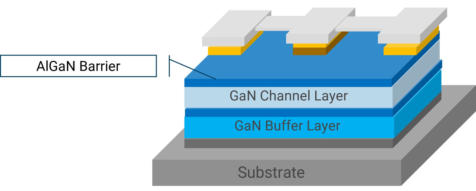
GaN HEMT structures

Key measurements:

  • AlGaN barrier thickness and composition
  • Strain vs relaxation
  • Interface roughness

Typical techniques:

  • HRXRD → strain + composition
  • XRR → thickness + roughness
  • XRF → elemental composition

Critical insight:

Electrical performance is strongly coupled to strain and interface quality; multi-technique fitting is required.

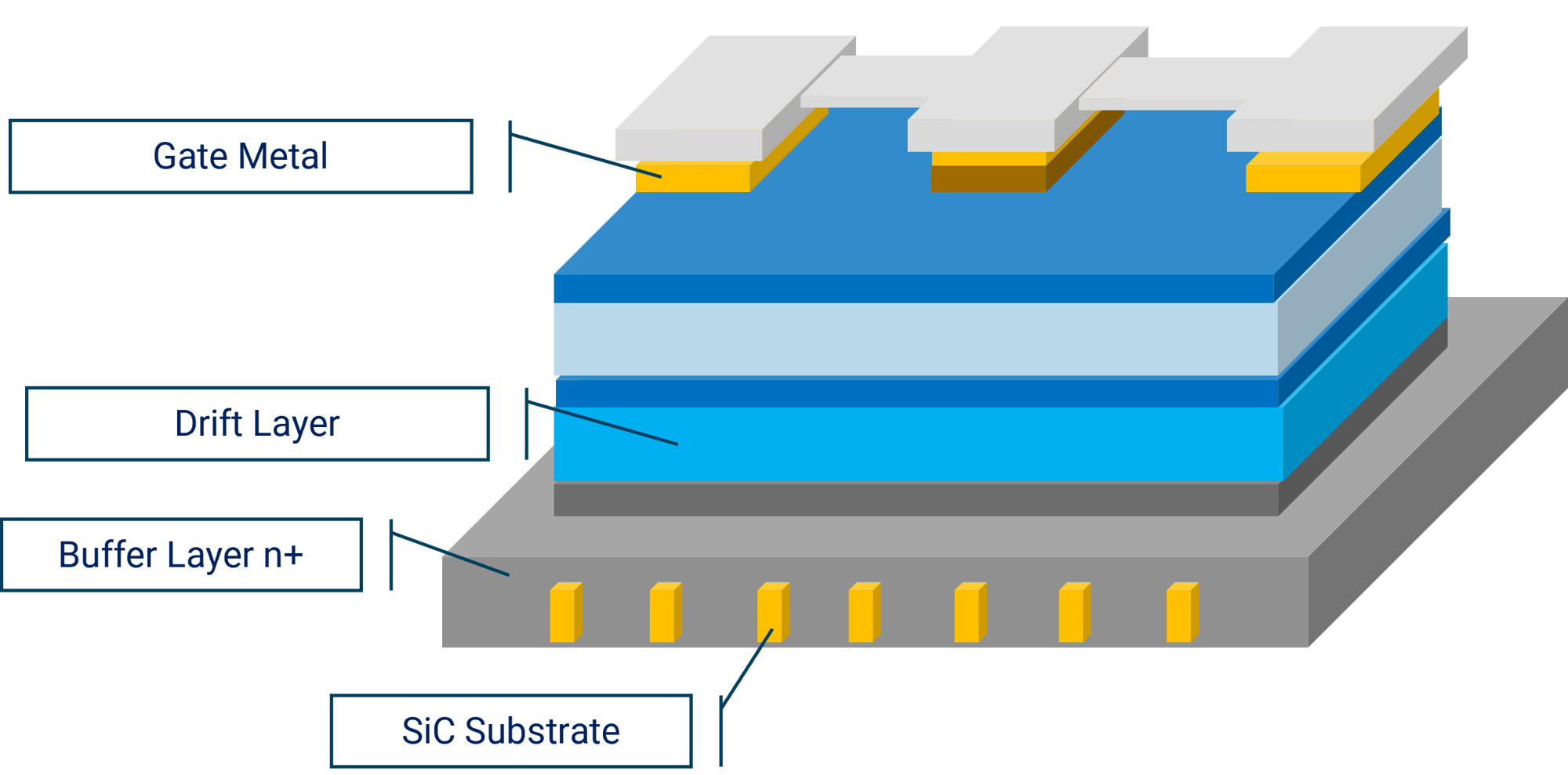
SiC power devices

Key measurements:

  • Substrate defect density
  • Epitaxial thickness uniformity
  • Polytype identification

Typical techniques:

  • X-ray topography → defects
  • HRXRD → crystal quality
  • XRF → composition

Critical insight:

Defect-driven yield loss requires non-destructive, wafer-scale inspection.

III–V epitaxy (InP, GaAs)

Key measurements:

  • Multilayer thickness
  • Lattice mismatch
  • Quantum well structures

Typical techniques:

  • HRXRD → strain and periodicity
  • XRR → thickness validation
  • XRT → defect inspection

Critical insight:

Inverse modeling becomes non-unique without constraints across multiple measurements.

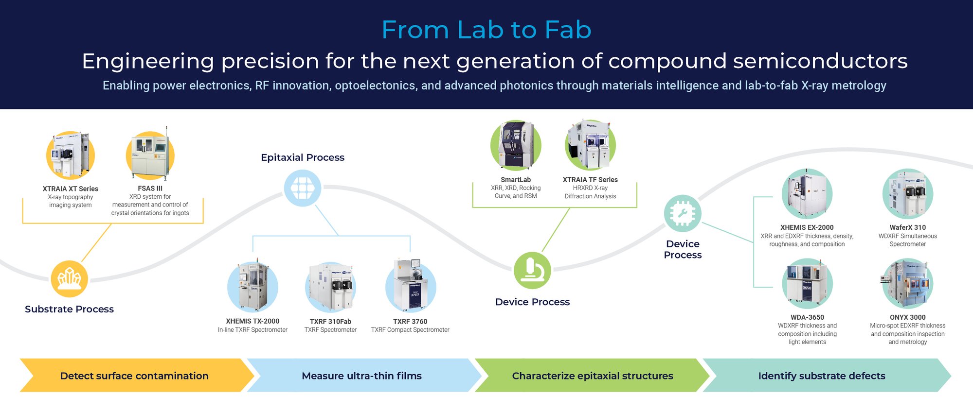
WU_26_RESE_CompoundSemiLandingPage_Graphics_11583832442_02_1920 x 817_

Our metrology solutions


Substrate

FSAS II

XRD system for measurement and control of crystal orientation for up to 150 mm wafers, ingots

Learn more
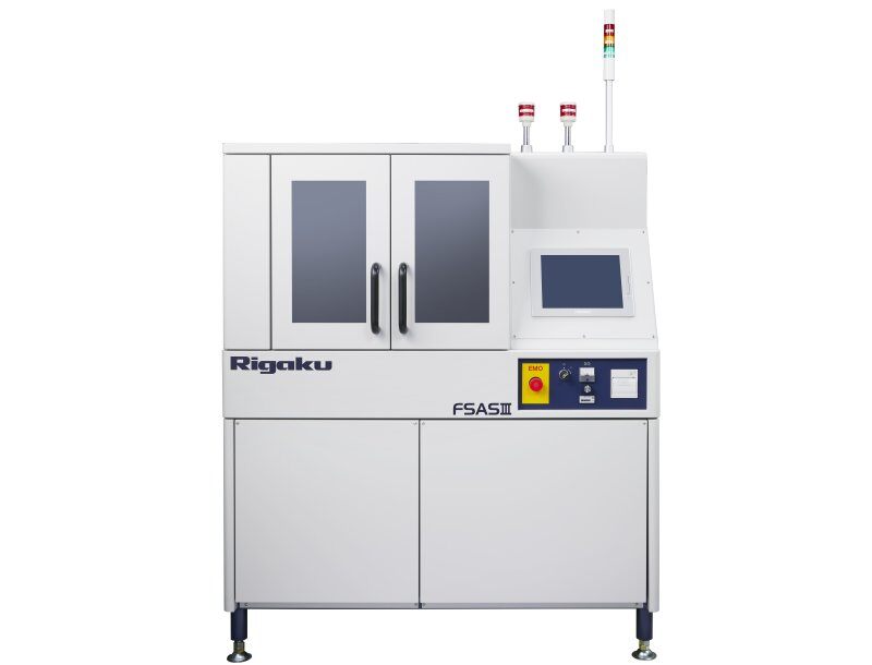
FSAS III

XRD system for measurement and control of crystal orientation for up to 150 mm wafers, ingots

Learn more
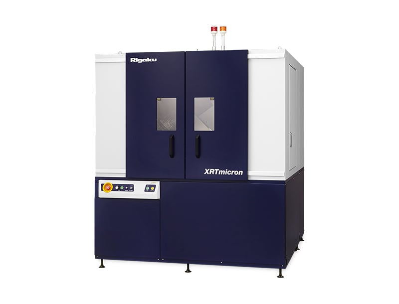
XRTmicron (Lab)

XRT (X-ray topography) imaging system for emerging power electronics, optoelectronics, and 5G / 6G communications (SiC, GaN, GaAs, InP, Ga₂O₃) for up to 300 mm wafers

Learn more
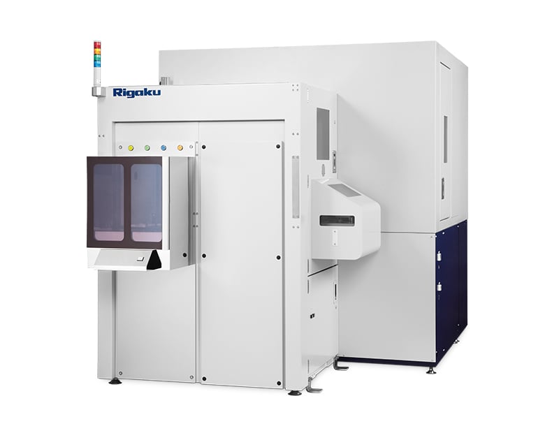
XRTmicron (Near-Fab)

XRTmicron (Near-Fab) bridging R&D and production

Learn more
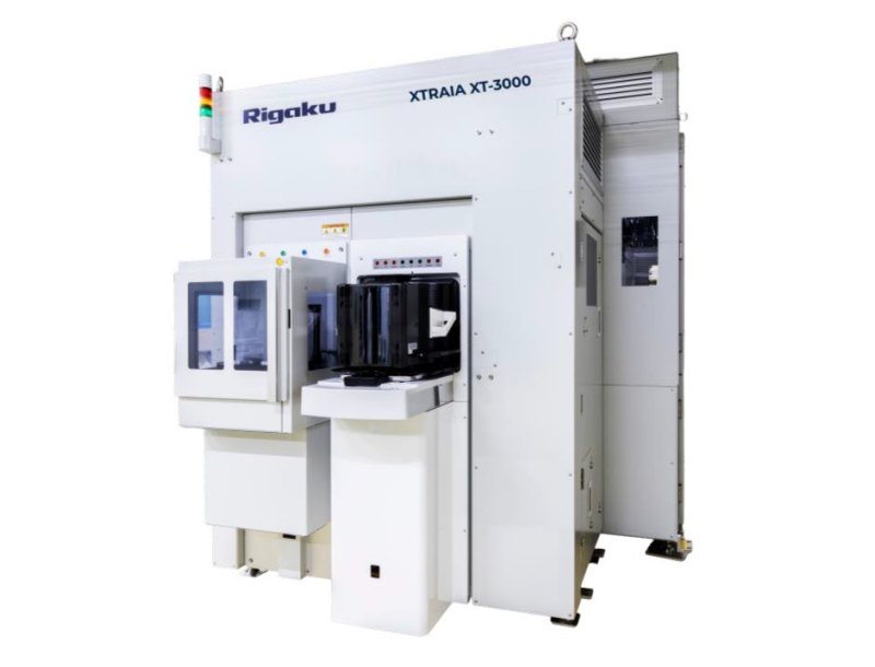
XTRAIA XT Series (Fab)

High-resolution, non-destructive wafer defect visualization for semiconductor manufacturing

Learn more

Epi

TXRF 3760

TXRF spectrometer for wafer surface contamination for up to 200 mm wafers

Learn more
XHEMIS TX-2000

Next-generation total-reflection XRF system for surface-metal control in semiconductor fabs for wafers up to 200 mm

Learn more
TXRF 310Fab

TXRF spectrometer for wafer surface contamination for up to 300 mm wafers

Learn more
TXRF-V310

TXRF-VPD spectrometer for wafer surface contamination for up to 300 mm wafers

Learn more

Device

SmartLab

Advanced, state-of-the-art, high-resolution XRD system powered by Guidance expert system software

Learn more
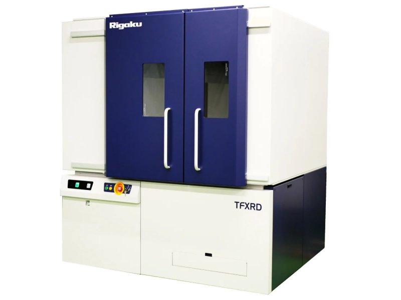
TFXRD Lab

HRXRD and XRR system for thickness, density, roughness, composition, strain, relaxation, and RSM characterization of unpatterned epitaxial films with full-wafer mapping capability for near-fab applications for up to 300 mm wafers

Learn more
TFXRD Near Fab

HRXRD and XRR system for thickness, density, roughness, composition, strain, relaxation, and RSM characterization of unpatterned epitaxial films with full-wafer mapping capability for near-fab applications for up to 200 mm wafers

Learn more
XTRAIA TF Series

High-resolution, non-destructive full-wafer characterization for thin film manufacturing

Learn more
XTRAIA XD-3300

XTRAIA XD-3300 HRXRD and XRR metrology tool for thickness, density, roughness, composition, strain, relaxation, and RSM characterization of unpatterned and patterned epitaxial films for up to 300 mm wafers

Learn more

Advanced packaging

WaferX 310

WDXRF simultaneous spectrometer for thickness and composition measurements for up to 300 mm wafers

Learn more
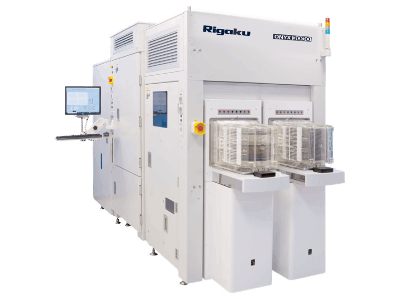
ONYX 3000

EDXRF and optical hybrid metrology tool for automated X-ray analysis, 3D scanning, and 2D microscope for film thickness and composition measurements on blanket and patterned wafers for up to 300 mm wafers

Learn more

Contact Us

Whether you are interested in getting a quote, want a demo, need technical support, or simply have a question, we're here to help.