Advanced X-ray Metrology Solutions for Photomask, Reticles, and Lithography Applications
Boost yield, minimize defects, and accelerate innovation with advanced X-ray and optical inspection tools for photomask and reticle processes
|
Accurate, non-destructive measurements |
Scalable from Lab to Fab |
Optimized for advanced device architectures |


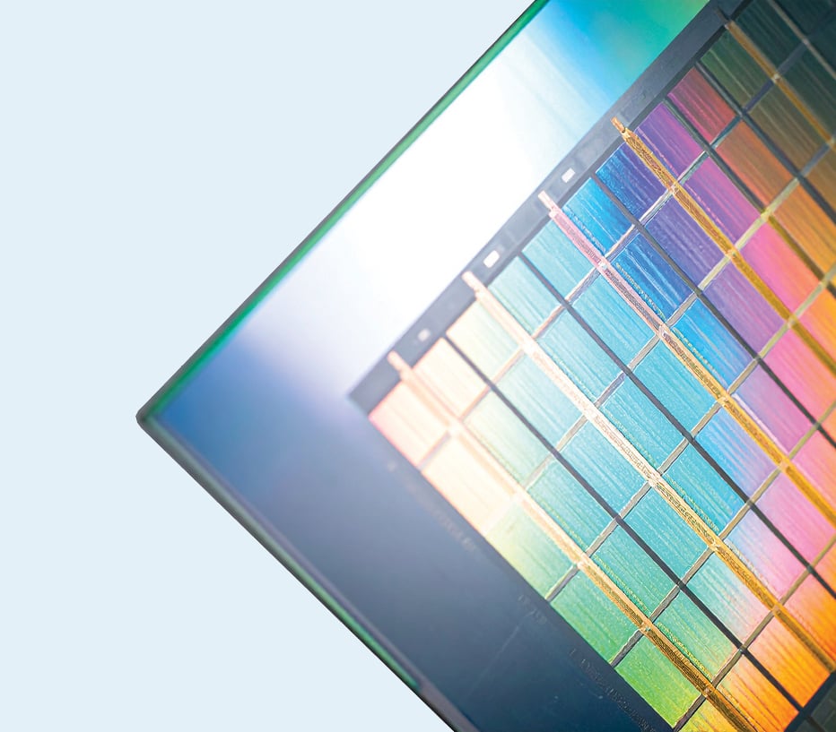
Rigaku’s Advanced X-ray Metrology Suite delivers non-destructive, high-precision analysis for EUV masks and high-aspect-ratio structures—from surface contamination to multilayer profiling and full-wafer mapping.
 XRR X-ray reflectometry |
 TXRF Total reflection X-ray fluorescence |
 TSAXS and GISAXS Transmission/Grazing incidence small angle X-ray scattering |
 XRF and XRD Integrated microspot analysis |
 Pattern recognition and recipe-based control systems for fab integration |
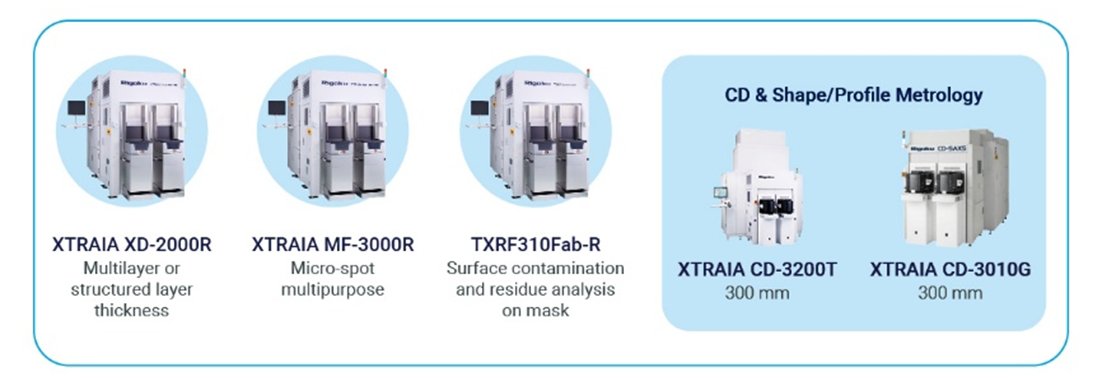
| Tool | Function | Description | Wafer size | Link |
|
XTRAIA XD-2000R
|
Layer thickness | Multilayer or structured layer thickness analysis using HRXRD/XRR with hybrid optics. | EUV Mask 152 x 152 x 6.35 mm |
View Product Page |
|
XTRAIA MF-3000R
|
Multi-purpose | Micro-spot platform for flexible thin film analysis, ideal for reticle and compound wafer R&D. | EUV Mask 152 x 152 x 6.35 mm |
View Product Page |
|
TXRF 310Fab-R
|
Surface analysis | Total reflection X-ray fluorescence (TXRF) for mask surface contamination and residue quantification. | EUV Mask 152 x 152 x 6.35 mm |
View Product Page |
|
XTRAIA CD-3200T
|
CD & shape metrology | High-resolution measurement of critical dimensions and topography for photomasks and wafers. | 300 mm | View Product Page |
|
XTRAIA CD-3010G
|
Profile metrology | Precision profiling and shape evaluation for advanced reticle and lithography structures. | 300 mm | View Product Page |


Contact Us
Whether you are interested in getting a quote, want a demo, need technical support, or simply have a question, we're here to help.