
EV_26_JSAP_LandingPageHero_11286628233_1200 x 300_

Rigaku at the 73rd JSAP Spring Meeting

Advanced X-ray Solutions for Semiconductor Innovation and Materials Research | March 15-16, 2026

Rigaku invites you to visit our exhibit at the 73rd JSAP Spring Meeting at the Institute of Science Tokyo, Ookayama Campus. Discover how our latest X-ray technologies enable faster development cycles, higher measurement confidence, and deeper structural insight—from semiconductor process development to advanced materials research.

Meet our specialists, explore application-focused solutions, and learn how Rigaku platforms support non-destructive analysis across R&D and manufacturing environments.

Schedule a Meeting with Rigaku at JSAP

JSAP Spring Meeting 2026 | Featured Lecture

Join us at the 73rd JSAP Spring Meeting 2026 in Tokyo for a technical presentation highlighting advanced X-ray diffraction approaches for next-generation nitride semiconductor structures. This session brings together expertise in crystallography, materials science, and device development, focusing on characterization methods that support innovation in ultraviolet optoelectronics.

[16p-PA3-8]  Multi-evaluation of AlN nanopillars using X-ray Diffraction Method 

Presenting Authors:
Taiji Yamamoto¹ , Weng Zhewei¹ , Takumu Saito² , Seiya Kato² , Sho Iwayama² , Motoaki Iwaya²  

¹ Rigaku Co., Ltd. | ² Meijo University

Keywords: Nitride semiconductors, X-ray diffraction, crystal growth

General Session (Poster Lecture)
15 Crystallography: 15.4 III-V Hydride Crystals
Session: [16p-PA3-1~11] 15.4 III-V Family Nitride Crystals
Date & Time: Monday, March 16, 2026 | 14:30 – 16:00
Location: PA3 (Arena, 1F)

Add to your calendar 

Overview

Ultraviolet lasers require operation at high currents and high powers, making vertical device structures advantageous. To achieve this structure, a delamination technique using pressurized hot water on nano-pillar-patterned AlN layers has been reported. The formation state of the AlN nano-pillars significantly affects the delamination characteristics and the crystallinity of the overlying AlGaN layer. This presentation reports on the results of the AlN nano-pillar layer evaluated using multiple analytical techniques based on X-ray diffraction method.

Visit our team

We welcome researchers, engineers, and collaborators interested in nitride materials, crystallography, and advanced X-ray metrology to attend the poster session and connect with our specialists to discuss challenges and opportunities in next-generation semiconductor development.

Semiconductor applications

Precision metrology for thin films, advanced packaging, and process development

Rigaku’s semiconductor-focused systems deliver high-precision structural characterization for thin films, epitaxy, and wafer-scale measurements. Designed for both research and in-line environments, these tools help accelerate device development while maintaining measurement accuracy.

Semiconductor metrology solutions: Benefits of advanced X-ray characterization

  • Non-destructive wafer characterization for rapid feedback without impacting valuable samples
  • High-resolution thin-film and epitaxy analysis to support advanced device architectures
  • High-throughput measurement workflows designed for modern fab environments
  • Scalable solutions that bridge R&D exploration and production-level process control

Request Semiconductor Application Consultation

XTRAIA XD-3300

XTRAIA XD-3300 HRXRD and XRR metrology tool for thickness, density, roughness, composition, strain, relaxation, and RSM characterization of unpatterned and patterned epitaxial films for up to 300 mm wafers

Learn more
XTRAIA CD-3200T

TSAXS metrology tool for critical dimension (CD) and profile shape characterization of deep (high aspect ratio) structures for 300 mm wafers

Learn more
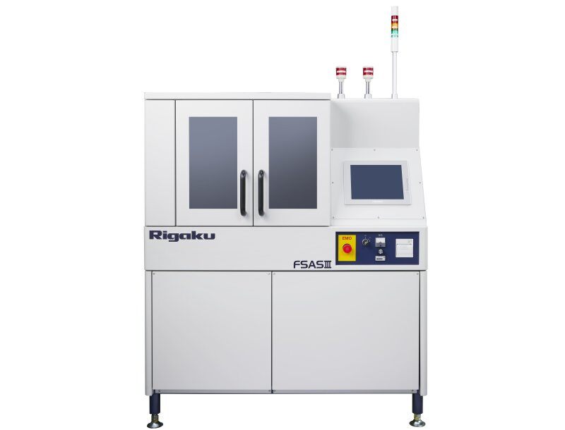
FSAS III

XRD system for measurement and control of crystal orientation for up to 150 mm wafers, ingots

Learn more
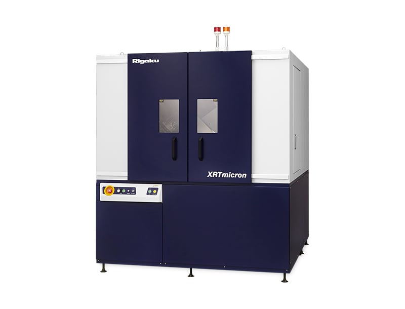
XRTmicron (Lab)

XRT (X-ray topography) imaging system for emerging power electronics, optoelectronics, and 5G / 6G communications (SiC, GaN, GaAs, InP, Ga₂O₃) for up to 300 mm wafers

Learn more
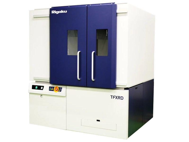
TFXRD Lab

HRXRD and XRR system for thickness, density, roughness, composition, strain, relaxation, and RSM characterization of unpatterned epitaxial films with full-wafer mapping capability for near-fab applications for up to 300 mm wafers

Learn more
TXRF 3760

TXRF spectrometer for wafer surface contamination for up to 200 mm wafers

Learn more

Short seminar - Japanese

Enhancing Semiconductor Device Reliability through Surface Metal Contamination Analysis | Surface Metal Analysis for SiC & GaN Devices

​Accurate detection of surface metal contamination is critical for ensuring semiconductor device performance, yield, and long-term reliability. As device geometries shrink and advanced materials such as SiC (Silicon Carbide) and GaN (Gallium Nitride) become mainstream in power semiconductor applications, the need for ultra-sensitive contamination analysis continues to grow.

This technical seminar introduces the TXRF3760 Total Reflection X-Ray Fluorescence (TXRF) Spectrometer, a high-sensitivity solution for surface metal contamination analysis in advanced semiconductor manufacturing environments.

Participants will learn how surface metal contamination impacts semiconductor device reliability, gain a clear understanding of the fundamentals of Total Reflection X-ray Fluorescence (TXRF) analysis, and explore the key features and advantages of the TXRF3760 system. The seminar will also present application examples for Si, SiC, and GaN devices, highlighting how TXRF supports process development and quality control.

This session is ideal for: semiconductor process engineers, contamination control and yield specialists, failure analysis and reliability engineers, as well as quality assurance and materials characterization professionals.

Date & time: March 16, 18:00​

Venue: 13.7 / W8E_101, Indoor Sports Hall​

Presenter: Hidetoshi Toda - Rigaku Corporation​

Topic: Overview of the surface metal contamination analysis system TXRF 3760​

​Join us to explore how advanced TXRF surface contamination analysis can strengthen semiconductor device reliability and support next-generation power device manufacturing. We look forward to welcoming you. 

Materials analysis applications

Flexible XRD platforms for research, education, and industrial materials development

Rigaku’s materials analysis solutions provide versatile diffraction capabilities for powders, thin films, and functional materials. From compact desktop systems to fully automated research platforms, these tools enable precise structural analysis across a wide range of applications.

Ideal applications

  • Functional materials and energy research
  • Thin films and coatings
  • Ceramics, catalysts, and powders
  • Academic and industrial laboratories
SmartLab

Advanced, state-of-the-art, high-resolution XRD system powered by Guidance expert system software

Learn more
SmartLab SE

Highly versatile multipurpose X-ray diffractometer with built-in intelligent guidance

Learn more
MiniFlex

Sixth-generation general purpose benchtop XRD system for phase ID and phase quantification

Learn more
SmartLab Studio II

Windows-based software suite for Rigaku's X-ray diffractometers

Learn more

Speak with a Materials Analysis Specialist

Experience Rigaku at JSAP

At our exhibit, you can:

  • Explore semiconductor-focused XRD and XRF solutions
  • See advanced reciprocal space mapping and XRD mapping technologies
  • Discuss real-world measurement challenges with application experts
  • Discover how automation and software integration streamline analysis workflows

Whether your focus is semiconductor metrology or materials research, Rigaku provides the precision and flexibility needed to move innovation forward.

Book a Meeting or Request Information

Planning to attend JSAP? Reserve time with our team to discuss your applications and see how Rigaku solutions can support your next breakthrough.

Contact Us

Whether you are interested in getting a quote, want a demo, need technical support, or simply have a question, we're here to help.