TFXRD Near Fab
High-resolution thin film XRF for RND and production environments
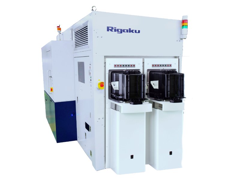
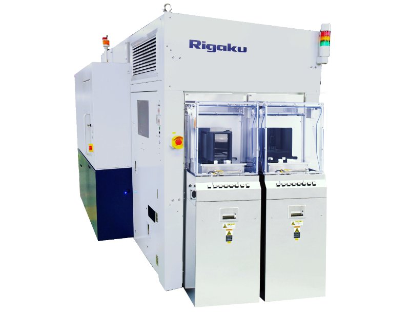
The Rigaku TFXRD Near-Fab brings lab-grade X-ray diffraction precision directly to semiconductor manufacturing lines. Designed for wafers up to 300 mm, this system enables fast, non-destructive analysis of epitaxial layers, thin films, and multilayer stacks through automated wafer handling and recipe-based operation. Its cleanroom-compatible design and high-throughput performance make it ideal for process qualification, defect detection, and yield optimization in the production of advanced power, RF, MEMS, and logic devices.
Available models:
- TFXRD Near-Fab 200: Supports wafers up to 200 mm
- TFXRD Near-Fab 300: Supports wafers up to 300 mm
TFXRD Near Fab Overview
The TFXRD Near-Fab is Rigaku’s versatile thin film X-ray diffraction system, engineered to bring high-resolution structural analysis directly into production environments. Designed for use near semiconductor fabrication lines, it enables rapid, non-destructive evaluation of epitaxial layers, thin film stacks, and multilayer heterostructures on wafers up to 300 mm.
With a compact, cleanroom-compatible footprint, automated wafer handling, and recipe-based operation, the TFXRD Near-Fab streamlines the transition from research and development (R&D) to pilot and high-volume manufacturing. It delivers precise measurements of lattice strain, crystal quality, layer thickness, composition, and orientation to support process qualification, early defect detection, and yield optimization.
By combining lab-grade accuracy with fab-level throughput, the TFXRD-300 ensures reliable monitoring and control of advanced thin film processes for power, RF, MEMS, and logic device production.
Pre-production & pilot lines (TFXRD Near-Fab)
- Recipe transfer from lab to fab environments
- Process qualification for new device architectures
- Semi-automated wafer characterization to support pilot runs
- Evaluation of defect density and layer uniformity before scale-up
- Early-stage monitoring of high-k/metal gate stacks and advanced dielectrics
TFXRD Near Fab Features
TFXRD Near Fab Specifications
| Technique | High-resolution thin film X-ray diffraction (HR-XRD) | |
|---|---|---|
| Purpose | Non-destructive structural analysis of epitaxial layers, thin films, and multilayer stacks | |
| Technology | High-precision θ-2θ goniometer with automated wafer alignment and recipe-based operation | |
| Key components | High-brilliance X-ray source; precision XRD optics; high-resolution 2D detector; cleanroom-ready enclosure | |
| Options | Automated wafer loader, environmental purge system, integrated curvature correction, SEMI-compliant software | |
| Wafer transfer / Sample handling | Automated wafer handling (supportsv200 mm and 300 mm wafers) | |
TFXRD Near Fab Events
Learn more about our products at these events
-
EventDatesLocationEvent website
-
The International Workshop on Gallium Oxide and Related Materials (IWGO-6)August 2 2026 - August 7 2026College Park, MD, USA.
-
SEMICON Taiwan 2026September 2 2026 - September 4 2026Taipei, Taiwan
-
ICSCRM Japan 2026 (Silver Sponsor)September 27 2026 - October 2 2026Yokohama, Japan
-
SEMICON West 2026October 13 2026 - October 15 2026San Francisco, CA, USA
-
SEMICON EuropaNovember 10 2026 - November 13 2026Munich, Germany
-
German Epitaxy WorkshopNovember 25 2026 - November 27 2026Freiburg, Germany
-
SEMICON Japan 2026December 9 2026 - December 11 2026Tokyo, Japan

Contact Us
Whether you are interested in getting a quote, want a demo, need technical support, or simply have a question, we're here to help.