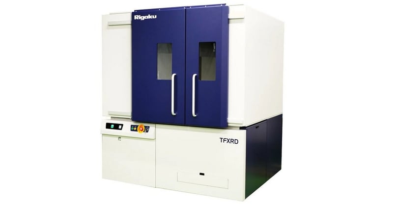
TFXRD Lab
Accelerate discovery with a compact, research-ready XRD platform. Ideal for universities and R&D labs developing new thin film materials and processes.
Learn more >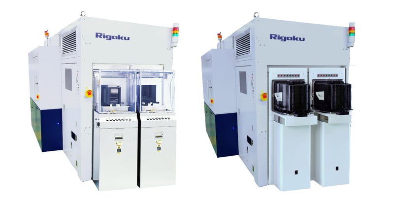
TFXRD Near-Fab
Bridge the gap between research and production. Semi-automated XRD metrology designed for recipe transfer, process qualification, and pilot-line readiness.
Learn more >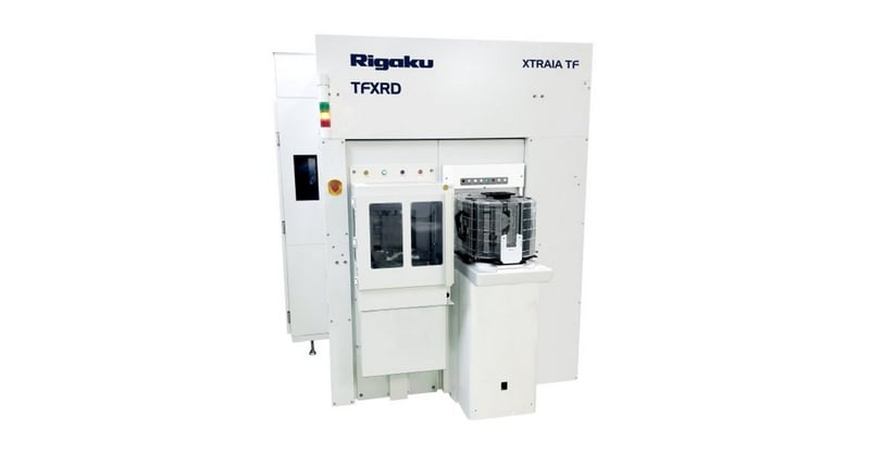
XTRAIA TF Series Fab
Fab-ready thin film XRD metrology for 200 mm and 300 mm wafers. SEMI-compliant, optimized for advanced logic, memory, and power devices.. Delivers high-throughput, automated thin film analysis for specialty fabs and mid-volume production.
Learn more >
Contact Us
Whether you are interested in getting a quote, want a demo, need technical support, or simply have a question, we're here to help.