XTRAIA XT Series (Fab)
X-ray topography that sees below the surface
High-resolution, Non-destructive wafer defect visualization for semiconductor manufacturing
The XTRAIA XT Series from Rigaku is the premier high-resolution X-ray topography (XRT) system designed for in-line detection of crystallographic defects across wafers and epitaxial layer stacks. By delivering full-wafer, non-destructive imaging with exceptional speed and precision, the XTRAIA XT Series enables fabs to achieve higher yield, improved process control, and long-term reliability in next-generation semiconductor devices.
Available models:
- XTRAIA XT-3000: Supports wafers up to 300 mm
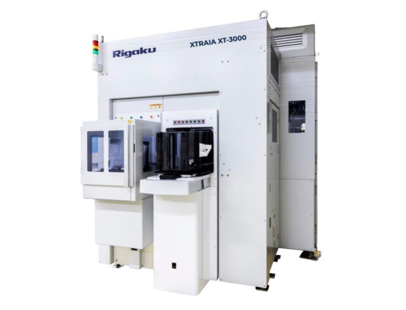
XTRAIA XT Series (Fab) Overview
Engineered for both R&D and high-volume manufacturing, the XTRAIA XT Series integrates seamlessly with fab workflows. Its cleanroom-ready design ensures compatibility with stringent contamination control requirements, while its automation capabilities—covering alignment, optics switching, and image acquisition—reduce operator workload and variability. Whether applied to silicon or advanced compound semiconductors (SiC, GaN, InP, GaAs, AlN, Ga₂O₃), the XTRAIA XT Series provides the resolution and repeatability required for advanced memory, logic, power, photonics, RF, and sensor applications.
The XTRAIA XT Series empowers semiconductor fabs to visualize dislocations, slip lines, and other crystallographic defects that threaten device performance. Built for full-wafer evaluation up to 300 mm, it ensures scalable yield management from lab to fab. Key benefits include:
- High-resolution, high-speed full-wafer imaging
- Non-destructive measurement with minimized particle or metal contamination
- Automation-ready system for in-line QC and R&D flexibility
- Wide material compatibility (Si, SiC, GaN, InP, GaAs, AlN, Ga₂O₃)
- SEMI S2/S8 compliant
- SECS/GEM and GEM300 compliant
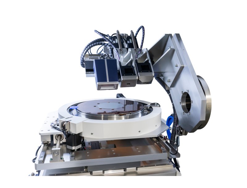
XTRAIA XT Series (Fab) Features
XTRAIA XT Series (Fab) Specifications
| Technique | X-ray topography imaging | |
|---|---|---|
| Purpose | Non-destructive evaluation of single-crystalline materials | |
| Technology | Switch between transmission and reflection topography | |
| Key components | High-brightness micro X-ray source; Specialized X-ray mirror optics; High-resolution, high-sensitivity X-ray camera; Transfer system | |
| Options | HR-XTOP camera, Crystal collimator, Defect inspection done with XRT Toolbox Software | |
| Wafer transfer / Sample handling | Supports automated wafer handling | |
| MiniEnvironment | Equivalent to ISO 14644-1 Class 6 | |
| SEMI Compliance | S2 / S8 / GEM300 | |
XTRAIA XT Series (Fab) Resources
Webinars
| Non-Destructive Dislocation Characterization in SiC Substrates Using XRTmicron Technology | Watch the Recording |
Rigaku Journal articles
| Read the Article | |
| Read the Article | |
| Read the Article | |
| Read the Article | |
| Read the Article |
Publications
XTRAIA XT Series (Fab) Events
Learn more about our products at these events
-
EventDatesLocationEvent website
-
The International Workshop on Gallium Oxide and Related Materials (IWGO-6)August 2 2026 - August 7 2026College Park, MD, USA.
-
SEMICON Taiwan 2026September 2 2026 - September 4 2026Taipei, Taiwan
-
ICSCRM Japan 2026 (Silver Sponsor)September 27 2026 - October 2 2026Yokohama, Japan
-
SEMICON West 2026October 13 2026 - October 15 2026San Francisco, CA, USA
-
SEMICON EuropaNovember 10 2026 - November 13 2026Munich, Germany
-
German Epitaxy WorkshopNovember 25 2026 - November 27 2026Freiburg, Germany
-
SEMICON Japan 2026December 9 2026 - December 11 2026Tokyo, Japan

Contact Us
Whether you are interested in getting a quote, want a demo, need technical support, or simply have a question, we're here to help.