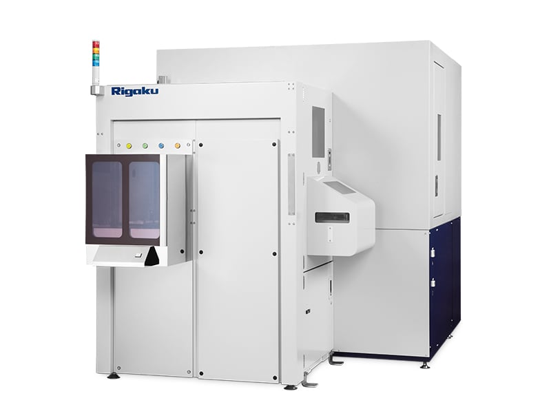
XRTmicron (Near-Fab)
Bridging R&D and production
X-ray topography solution for seamless transition from Lab to Fab
The XRTmicron (Near-Fab) system is Rigaku’s hybrid solution for semiconductor manufacturers who need a flexible tool that serves both research and pilot production lines. By offering both manual and automated wafer transfer, the Near-Fab configuration delivers the versatility required for evolving workflows.
Engineered for minimized contamination,, non-destructive wafer evaluation, the system supports a wide range of wafer sizes (75–300 mm) and substrates, including Si, SiC, GaN, GaAs, InP, AlN, and Ga₂O₃. With advanced optics, detectors, and 3D cross-section topography capabilities, the XRTmicron (Near-Fab) ensures precise defect visualization while preparing processes for fab-scale deployment.
XRTmicron (Near-Fab) Overview
The XRTmicron (Near-Fab) is designed for semiconductor manufacturers who require a flexible evaluation system that works across both R&D environments, pilot production lines, and high-volume production. Positioned between the Lab and Fab configurations, it combines research-level precision with the automation and reliability needed for process integration and quality control.
Supporting wafers up to 300 mm, the Near-Fab system offers both manual and automated wafer transfer, making it ideal for fabs in transition—from early material studies to process qualification and in-line quality monitoring. Its non-destructive, high-resolution imaging provides detailed visualization of dislocations, slip lines, and other crystallographic defects that directly impact device yield and reliability.
With SEMI-compliant defect analysis software, the XRTmicron (Near-Fab) enables engineers to bridge the gap between discovery and high-volume manufacturing, ensuring that materials and processes are production-ready.
Applications
- SiC for power devices: TSD and BPD mapping (SEMI M91/M93 compliant)
- GaN & AlN for RF, optoelectronics and power devices: Process development and quality control
- InP & GaAs for VCSEL and photonics: defect mapping on substrate and epi-level
- Ga₂O₃ for power devices: Substrate and epitaxy quality improvement
- Al₂O₃ as optoelectronic substrates: process improvement and quality control
- Si/SiGe superlattices for 3D-DRAM and advanced logic structures: Process development and misfit dislocation detection
XRTmicron (Near-Fab) Features
XRTmicron (Near-Fab) Specifications
| Technique | X-ray topography imaging | |
|---|---|---|
| Purpose | Non-destructive evaluation of single-crystalline materials | |
| Technology | Switch between transmission and reflection topography | |
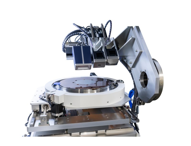
| Key components | High-brightness micro X-ray source; Specialized X-ray mirror optics; High-resolution, high-sensitivity X-ray camera; Transfer system | |
| Options | HR-XTOP camera, Crystal collimator,Defect inspection done with XRT Toolbox Software | |
| Wafer transfer / Sample handling | Supports both automated and manual wafer handling | |
XRTmicron (Near-Fab) Resources
Webinars
| Non-Destructive Dislocation Characterization in SiC Substrates Using XRTmicron Technology | Watch the Recording |
Rigaku Journal articles
| Read the Article | |
| Read the Article | |
| Read the Article | |
| Read the Article | |
| Read the Article |
Publications
XRTmicron (Near-Fab) Events
Learn more about our products at these events
-
EventDatesLocationEvent website
-
The International Workshop on Gallium Oxide and Related Materials (IWGO-6)August 2 2026 - August 7 2026College Park, MD, USA.
-
SEMICON Taiwan 2026September 2 2026 - September 4 2026Taipei, Taiwan
-
ICSCRM Japan 2026 (Silver Sponsor)September 27 2026 - October 2 2026Yokohama, Japan
-
SEMICON West 2026October 13 2026 - October 15 2026San Francisco, CA, USA
-
SEMICON EuropaNovember 10 2026 - November 13 2026Munich, Germany
-
German Epitaxy WorkshopNovember 25 2026 - November 27 2026Freiburg, Germany
-
SEMICON Japan 2026December 9 2026 - December 11 2026Tokyo, Japan

Contact Us
Whether you are interested in getting a quote, want a demo, need technical support, or simply have a question, we're here to help.