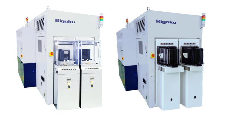
TFXRD Systems
From Lab to Fab: Scalable thin film XRD solutions for every stage of semiconductor manufacturing.
The TFXRD & XTRAIA TF Series deliver unmatched thin film XRD metrology, from research labs to high-volume fabs. With solutions tailored for R&D, pilot lines, and full-scale production, this portfolio ensures consistent, non-destructive analysis of thin film structure, strain, stress, and thickness. Whether advancing new materials or optimizing manufacturing yield, Rigaku provides a clear pathway from Lab → Near-Fab → Fab.
TFXRD & XTRAIA TF series features
- Non-destructive thin film metrology – Comprehensive X-ray diffraction (XRD), reflectivity (XRR), and reciprocal space mapping (RSM) in one platform.
- Full-wafer capability – Supports wafers up to 200 mm and 300 mm depending on model, enabling seamless scale-up from research to high-volume
- High-resolution detectors – Equipped with Rigaku’s HyPix detector technology for superior data accuracy, speed, and dynamic
- Material flexibility – Ideal for analyzing wide bandgap semiconductors (SiC, GaN, GaN-on-Si), advanced dielectrics, III–V compounds, and multilayer heterostructures.
- Process insight – Delivers key parameters such as strain, stress, crystallinity, thickness, density, interface quality, and defect
- Scalability – Portfolio designed to bridge the gap between R&D labs, pilot lines, and fab production, ensuring consistency across development cycles.
- Recipe-driven workflows – Simplified, repeatable measurement routines with customizable recipes for faster process qualification.
- Cleanroom-ready design – All systems engineered for semiconductor environments, with automation scaling from manual handling (Lab) to full fab automation (Fab).
- Compact footprint – Optimized system design to fit space- constrained labs and fab cleanrooms.
- Future-ready integration – Compatible with fab automation protocols (SECS/GEM, GEM300) to support digital factory
Products
TFXRD Lab
Accelerate discovery with a compact, research-ready XRD platform. Ideal for universities and R&D labs developing new thin film materials and processes.
Learn more >
TFXRD Near-Fab
Bridge the gap between research and production. Semi-automated XRD metrology designed for recipe transfer, process qualification, and pilot-line readiness.
Learn more >XTRAIA TF Series Fab
Fab-ready thin film XRD metrology for 200 mm and 300 mm wafers. SEMI-compliant, optimized for advanced logic, memory, and power devices.. Delivers high-throughput, automated thin film analysis for specialty fabs and mid-volume production.
Learn more >Applications
|
Research & Development
|
Pre-Production & Pilot Lines
|
|
200 mm Fab Production
|
300 mm High-Volume Fab Production
|
Which thin film XRD system fits your needs?
| System | TFXRD Lab | TFXRD Near-Fab | XTRAIA TF (Fab) |
| Maximum wafer size | 300 mm | 300 mm | 300 mm |
| Sample handling | Manual | Auto + Manual | Fully Automated |
| MiniEnvironment (with FFU) | N/A | N/A | ISO Class 6 equivalent |
| Wafer ID OCR | No | Optional | Standard |
| Purpose | Lab, R&D, material studies | R&D, pilot line, process dev, production QC | Full SEMI fab QC, high-volume yield |
| SEMI (S2/S8) Compliance | No | No | Yes |
| SECS/GEM and GEM300 | No | Optional | Yes |

Contact Us
Whether you are interested in getting a quote, want a demo, need technical support, or simply have a question, we're here to help.
