Semiconductor and Electronic Devices

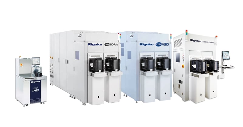
TXRF series
Total reflection X-ray fluorescence
TXRF series metrology tools offer significant advantages in semiconductor manufacturing and R&D to evaluate surface contamination. Non-destructive TXRF measurements are highly sensitive to trace elements, including Na, Mg, and Al, transition metals, and heavy elements. Integrated Vapor-Phase Decomposition (VPD) capability available in the TXRF-V310 and XHEMIS TX-3000V enables the lowest detection limits. They are sensitive to trace elements, highly sensitive, and capable of quantitative analysis. These non-destructive tools excel in analyzing thin films, provide valuable insights into their elemental composition and thickness, and contribute to enhanced quality control, optimized processes, and a deeper understanding of materials. Rigaku metrology solutions: TXRF 3760, TXRF 310Fab, TXRF-V310, XHEMIS TX-3000, and XHEMIS TX-3000V.
Learn more >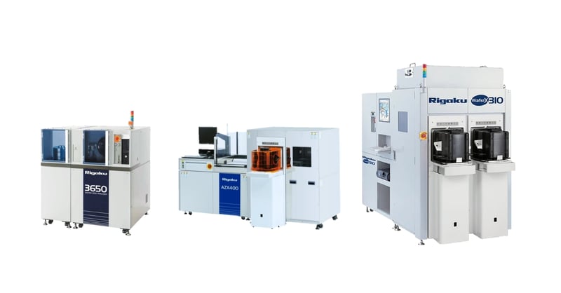
WDXRF series
Wavelength dispersive X-ray fluorescence
The WDXRF series is known for its exceptional precision and accuracy in measuring the thickness and composition of materials, particularly with light elements. Becoming invaluable instruments in both semiconductor manufacturing and R&D, where maintaining strict control over material properties is crucial for creating high-performance semiconductor devices. Rigaku metrology solutions: AZX 400, WDA-3650, and WaferX 310.
Learn more >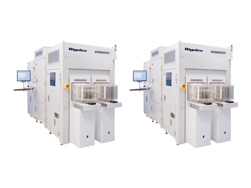
ONYX series
Hybrid energy dispersive X-ray fluorescence and optical techniques
Typically for characterization of multilayered samples for BEOL and packaging applications. It combines micro-spot EDXRF, 2D microscope, and 3D scanner for in-line, non-destructive inspection and metrology. Rigaku metrology solutions: ONYX 3000 and ONYX 3200.
Learn more >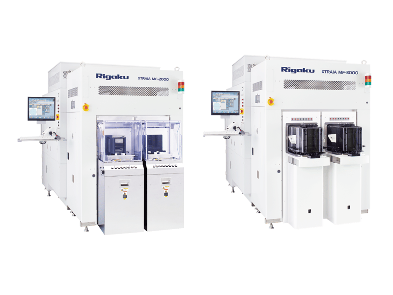
XTRAIA MF series
EDXRF (Energy dispersive X-ray fluorescence), XRR (X-ray reflectivity), and XRD (X-ray diffraction
The combination of X-ray techniques supports a wide range of applications typically for the characterization of ultrathin, multilayer samples, blanket, and patterned wafers. Rigaku metrology solutions: XTRAIA MF-2000 and XTRAIA MF-3000
Learn more >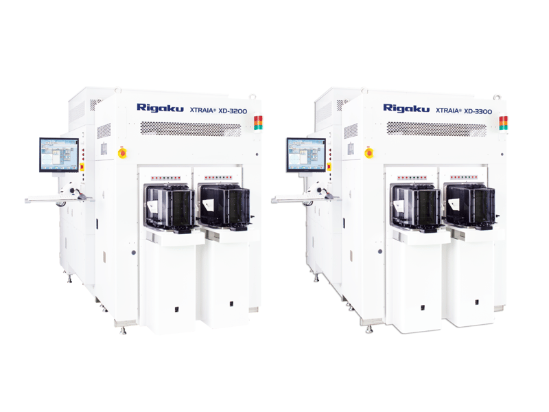
XTRAIA XD series
HRXRD (high-resolution X-ray diffraction) and XRR
Strain, composition, and thickness of epitaxial layers, crystalline phase, and texture of polycrystalline films. Thin film and film stack thicknesses and density. Rigaku metrology solutions: XTRAIA XD-3200 and XTRAIA XD-3300
Learn more >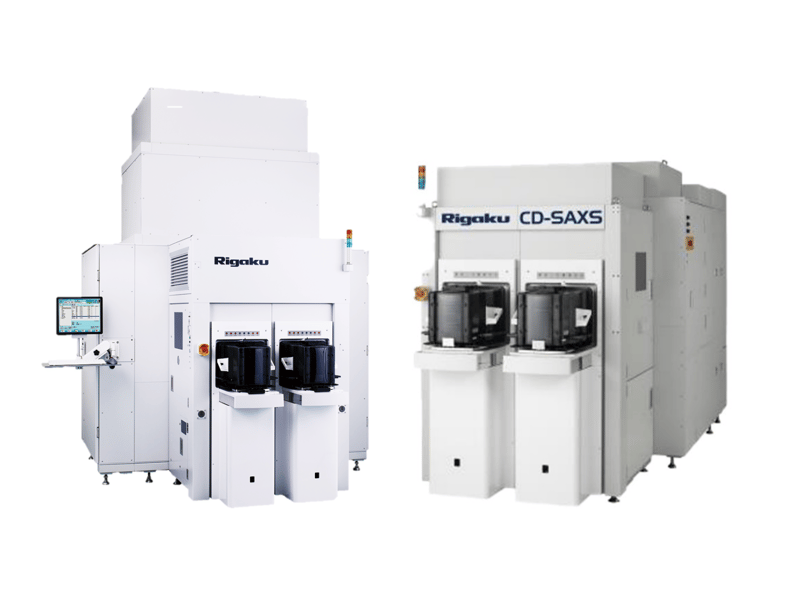
XTRAIA CD series
CDSAXS: X-ray CD metrology tools for grazing incidence and transmission measurements for up to 300 mm
GISAXS for in-line small angle scattering for shallow CD measurements XTRAIA CD-3200G. TSAXS for in-line small angle X-ray scattering for high aspect ratio device CD measurements XTRAIA CD-3200T.
Learn more >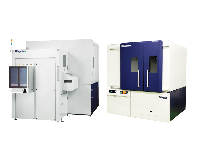
Near-fab metrology solutions
In-line monitoring and control of various processes to ensure the quality and consistency of semiconductor devices. Typically located in close proximity to the fabrication (fab) area. The near-fab metrology tools play a key role in ensuring the quality, consistency, and reliability of semiconductor manufacturing processes. Enabling monitoring and feedback, to optimize manufacturing parameters and enhance overall yield. Understand crystallographic defects by X-ray topography and thin film properties by X-ray diffraction with Rigaku metrology solutions: XRTmicron, and TFXRD SERIES.
Learn more >
XRTmicron Series
High-resolution X-ray topography platform, engineered to detect and quantify crystallographic defects in single-crystal wafers and epitaxial layers. With configurations for R&D labs, pilot lines, and full-scale fabs, it enables end-to-end defect visualization and yield optimization. Combining non-destructive measurement, cleanroom compatibility, and advanced automation, the system delivers accurate defect maps and statistical dislocation analysis, bridging research innovation and manufacturing reliability for improved device performance.
Learn more >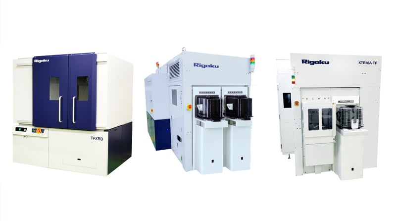
TFXRD Series
Scalable thin film XRD solutions for every stage of semiconductor manufacturing.
The XTRAIA TF Series delivers precise, non-destructive thin film XRD metrology from research labs to high-volume fabs. Covering R&D, pilot lines, and full production, it enables accurate analysis of structure, strain, stress, and thickness to accelerate innovation and ensure yield stability. With TFXRD Lab for flexible materials research, TFXRD Near-Fab for automated process development, and XTRAIA TF Fab for high-throughput in-line monitoring, Rigaku provides a clear pathway from lab to fab.

Contact Us
Whether you are interested in getting a quote, want a demo, need technical support, or simply have a question, we're here to help.