
Non-destructive Characterization of Crystallographic Defects of SiC Substrates using X-ray Topography for R&D and Quality Assurance in Production

Christian Reimann and Christian Kranert

Summer 2021 Volume 37, No. 2 , 33-37

One of the major technical challenges of this decade are energy efficient technologies, which is among others, comparable in its importance to Artificial Intelligence, 5G and IoT. Innovative silicon carbide (SiC) technology and components will contribute significantly towards the goal of a greener, energy efficient and sustainable economy. SiC also addresses major and dynamic growth markets such as renewable energy generation and conversion, edge computing, cloud computing and data centers and last but not least the imminent change to and corresponding growth of electric mobility solutions. SiC is therefore one of the most important semiconducting material in this decade.

Due to the current undersupply of SiC substrates, the obtained prices for typical 150 mm n-type SiC wafers are quite high and in the range of $800–$1200 per wafer, depending on the material quality and the purchased quantity. Beside wafer prices, the material quality is a very important factor to choose the right material supplier. A stable baseline, instead of handpicking small numbers of best case wafers, for supplying high quality SiC substrates is needed to manufacture reliable SiC power devices, which is especially requested for automotive application. Therefore, a strong need for non-destructive and reliable SiC substrate characterization occurs, which supports R&D purposes, e.g. defect optimization or scale up to 200 mm substrate diameter, and of course in-line capability in terms of quality assurance within production environment.
Highlights

  • X-ray topography enables rapid, non-destructive mapping of crystallographic defects across entire SiC wafers, supporting both research and high-throughput production quality assurance.
  • Automated defect detection algorithms can quantify threading screw dislocation (TSD) densities on 150 mm wafers in minutes while achieving accuracy comparable to manual inspection.
  • Optimized partial-wafer measurement strategies significantly reduce inspection time while maintaining acceptable accuracy for industrial process control.

Summary

Silicon carbide (SiC) has become a critical semiconductor material for electric vehicles, renewable energy systems, fast charging infrastructure, and other high-power electronic applications. As demand increases, manufacturers require reliable methods to evaluate substrate quality because crystallographic defects directly affect epitaxial growth, device yield, long-term reliability, and production costs. Traditional defect characterization techniques have limitations, particularly for heavily doped substrates and production-scale inspection.

Lab-based X-ray topography provides a non-destructive approach for imaging and quantifying crystallographic defects across entire SiC wafers. The technique can identify important defect types including threading screw dislocations (TSDs), basal plane dislocations (BPDs), micropipes, stacking faults, and other structural imperfections that influence device performance. Automated image analysis algorithms enable rapid defect detection and density mapping, reducing analysis time while maintaining accuracy comparable to manual evaluation.

For TSD analysis, automated processing can evaluate a full 150 mm wafer in less than five minutes after image acquisition, producing detailed defect density maps that reveal spatial variations across the wafer. Measurement strategies can be adapted for manufacturing environments by analyzing selected grid or stripe regions instead of performing full-wafer scans. Grid-based sampling provides a favorable balance between inspection speed and measurement accuracy, making it well suited for routine quality assurance.

The same X-ray topography approach is also being extended to quantify BPDs, micropipes, stacking faults, and threading edge dislocations. Correlation with established characterization methods demonstrates that the technique provides reliable defect measurements while eliminating destructive sample preparation. These capabilities support substrate optimization, process development, and production quality control throughout the SiC manufacturing process, helping improve wafer quality and ultimately increasing the yield and reliability of power semiconductor devices.

Frequently asked questions

Recommended products

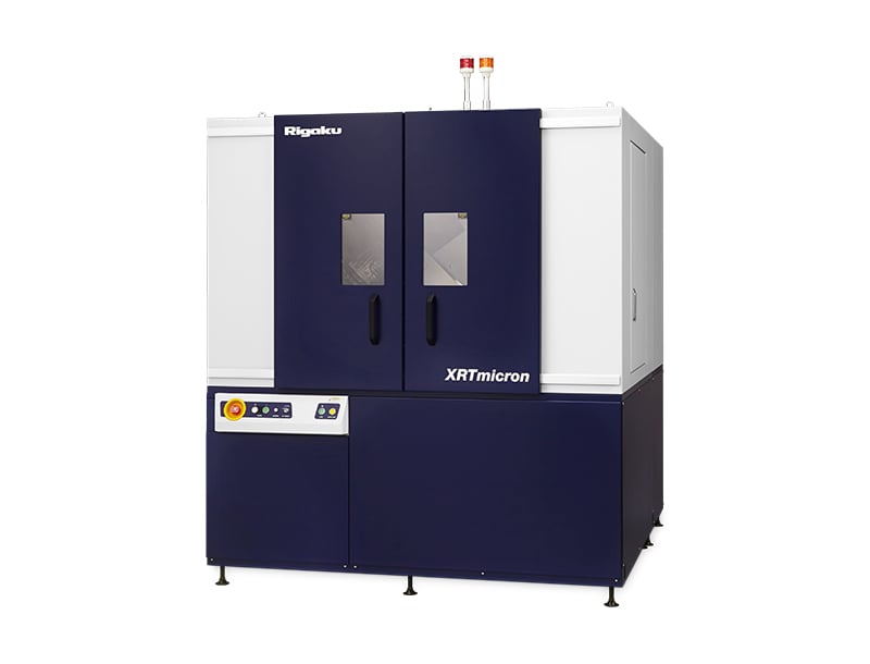
XRTmicron (Lab)

XRT (X-ray topography) imaging system for emerging power electronics, optoelectronics, and 5G / 6G communications (SiC, GaN, GaAs, InP, Ga₂O₃) for up to 300 mm wafers

Learn more

Subscribe to Understanding Semiconductors newsletter

Connect with semiconductor leaders in metrology, process, and analytics to solve your biggest metrology challenges.

Contact Us

Whether you are interested in getting a quote, want a demo, need technical support, or simply have a question, we're here to help.