
| Tool | Function | Description | Wafer size | Link |
XTRAIA XD-2000R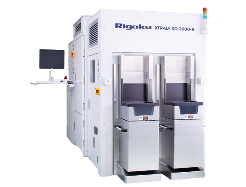 |
Layer thickness | Multilayer or structured layer thickness analysis using HRXRD/XRR with hybrid optics. | EUV Mask 152 x 152 x 6.35 mm |
View Product Page |
XTRAIA MF-3000-R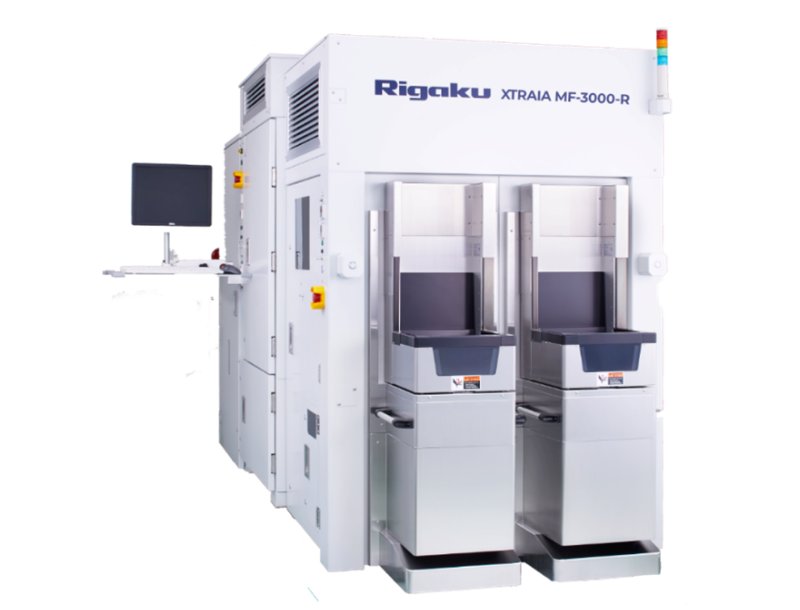 |
Multipurpose | Microspot platform for flexible thin film analysis, ideal for reticle and compound wafer R&D. | EUV Mask 152 x 152 x 6.35 mm |
View Product Page |
TXRF 310Fab-R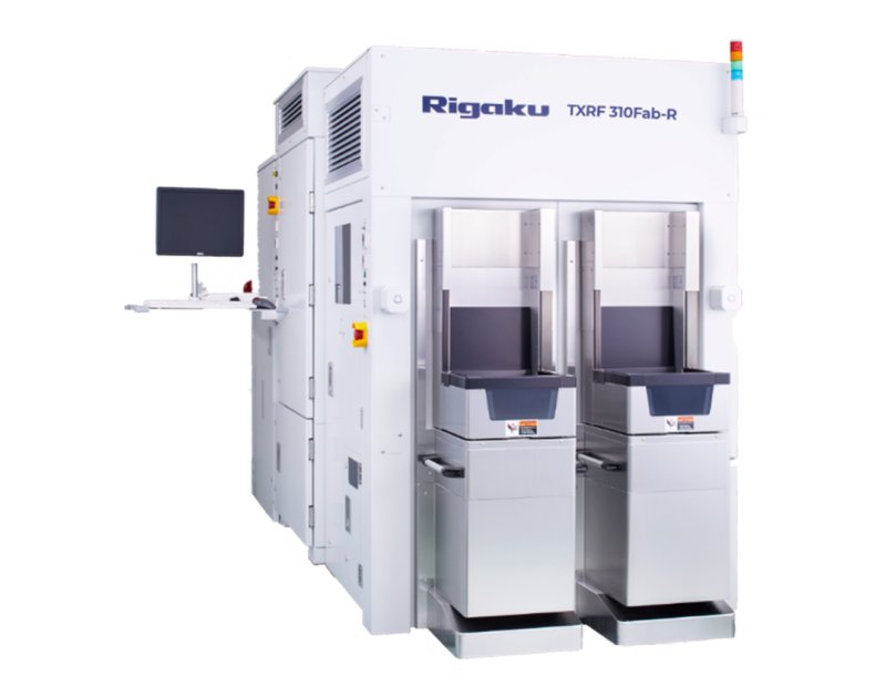 |
Surface analysis | Total reflection X-ray fluorescence (TXRF) for mask surface contamination and residue quantification. | EUV Mask 152 x 152 x 6.35 mm |
View Product Page |
XTRAIA CD-3200T |
CD & shape metrology | High-resolution measurement of critical dimensions and topography for photomasks and wafers. | 300 mm | View Product Page |
XTRAIA CD-3010G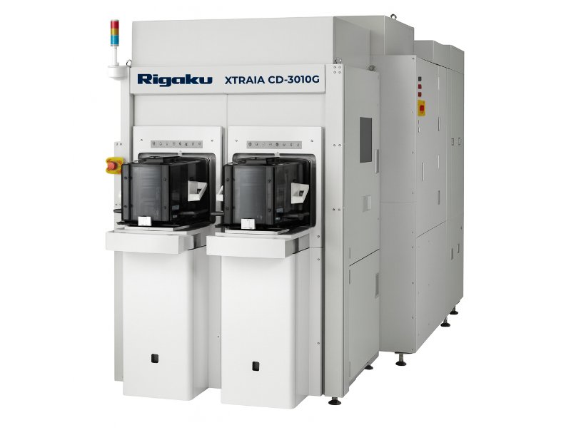 |
Profile metrology | Precision profiling and shape evaluation for advanced reticle and lithography structures | 300 mm | View Product Page |

Contact Us
Whether you are interested in getting a quote, want a demo, need technical support, or simply have a question, we're here to help.