Semicon Japan 2026 header
Dates and venue
December 9–11, 2026 · Tokyo Big Sight
Booth
Silver Sponsor · E2433
Portfolio
XRF · XRD · XRR · SAXS · TXRF · X-ray imaging

Rigaku Semiconductor Metrology

Confidence for every critical layer

Scaling, 3D architectures and heterogeneous integration create measurement challenges that cannot be solved by surface-only insight. Rigaku combines deep X-ray expertise with production-ready automation to reveal the composition, structure, thickness and contamination that determine device performance and yield.

75+
Years of X-ray innovation
300 mm
Production-ready solutions
Non-destructive
Insight into buried structures
Lab to Fab
Connected measurement workflow
Featured at the booth

Solutions for the devices shaping tomorrow

Discover a complete portfolio for IoT, advanced logic and memory, advanced packaging, and power semiconductors.

Process map

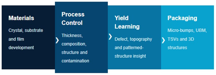
One partner across the semiconductor value chain

Turn materials intelligence into reliable process control with a measurement portfolio engineered to follow your product from technology development to yield learning.

Talk with Rigaku application specialists about a solution designed for your material, process and production environment. See how non-destructive X-ray analysis delivers the clarity to accelerate learning and improve yield.

Find us at Booth E2433


SemiconJapan image 1
SemiconJapan image 2


IOT devices

IOT devices · WDXRF

AZX 400 & WDA-3650

Film thickness and film-type analysis across development and production.

IOT devices · XRF

XHEMIS EX-2000

200 mm-compatible film thickness metrology from process development to quality control.

Advanced devices

Advanced devices · TXRF

TXRF-V310

300 mm metal contamination monitoring and evolving VPD contamination analysis.

Advanced devices · TXRF

XHEMIS TX-3000

Ultra-fast mapping for instant metal contamination analysis. By combining high-performance hardware with AI analysis, overall analysis performance can be improved by up to six times.

Advanced devices · WDXRF

WaferX 310

Film thickness measurement for advanced device process control.

Advanced devices · X-ray metrology

XTRAIA MF Series

Inline composition analysis and X-ray metrology for semiconductor process control.

Advanced devices · XRD / XRR

XTRAIA XD-3300

Semiconductor inline XRD/XRR, including SiGe film thickness measurement.

Advanced devices · SAXS

XTRAIA CD Series

Non-destructive patterned-structure and deep-hole measurement using GI-SAXS, LE GI-SAXS and T-SAXS.

Advanced packaging

Advanced packaging · micro-spot XRF

ONYX 3200

Ultra-small-area thickness and composition measurement with dual-beam X-ray optics.

Advanced packaging · X-ray imaging

XHENA AX-3000

Non-destructive inspection of micro-bump and TSV defects.

Advanced packaging · X-ray CT

CT Lab HR160

High-resolution 3D inspection for complex packaging structures.

Power devices

Power devices · TXRF

TXRF3760 & XHEMIS TX-2000

SiC measurement applications and next-generation contamination analysis.

Power devices · X-ray metrology

WDXRF & XRTmicron

Dopant concentration, film thickness and advanced X-ray topography analysis.

Power devices · XRD

XTRAIA XT / TF / OR

From R&D through manufacturing: XRD mapping, QC and crystal orientation solutions.

Contact Us

Whether you are interested in getting a quote, want a demo, need technical support, or simply have a question, we're here to help.