Is wafer-level packaging an issue for your semiconductor manufacturing process?
Elevate your wafer inspection and metrology processes with the ONYX Series, where precision meets innovation.
Layer-by-layer wafer inspection with qualitative and quantitative results
Click on the video to learn more.
ONYX 3000
IN-LINE NON-DESTRUCTIVE WAFER INSPECTION AND METROLOGY
Hybrid configuration
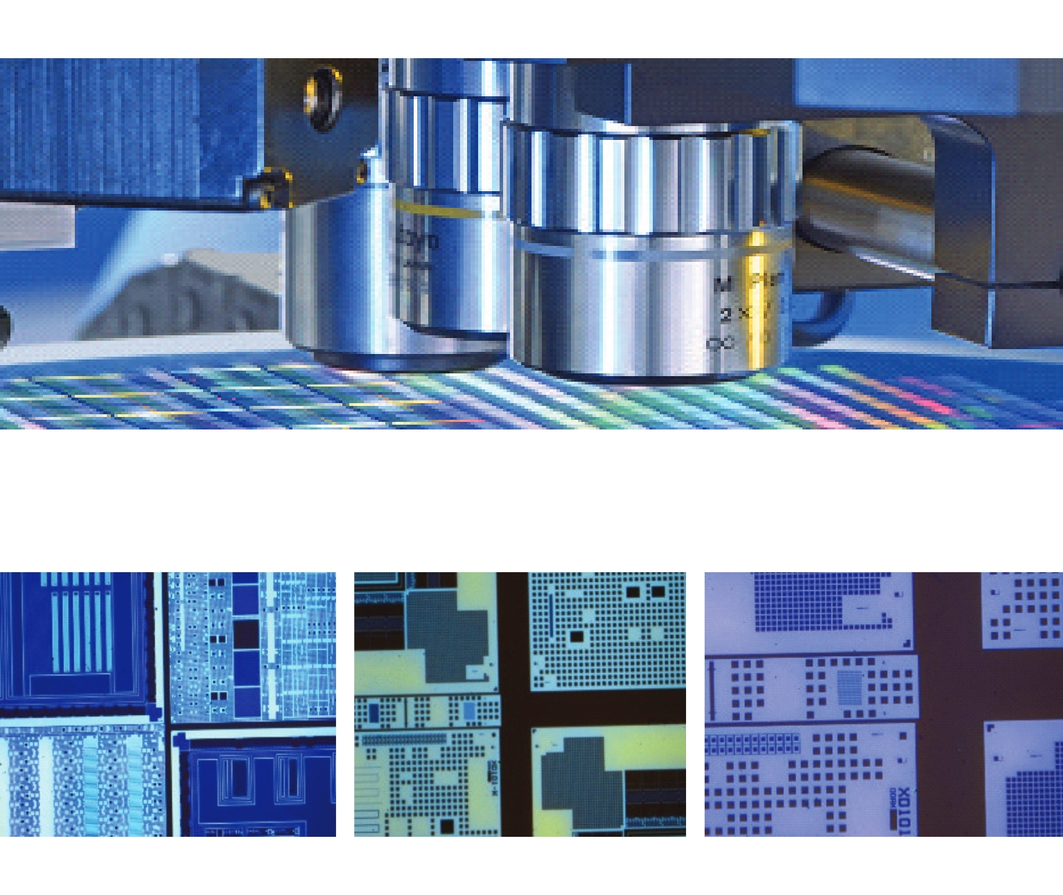
Automated X-ray Analysis, 3D scanning, and 2D microscope for film thickness and composition measurements on blanket and patterned wafers
2D microscope

2D microscope magnification

3D scanner

Configurable for 300 mm and smaller wafers

ONYX 3000 Advantages
Layer-by-layer wafer inspection with qualitative and quantitative results
- XRF measures elemental composition and film thickness
- 2D Microscope used for pattern recognition, and CD calculation.
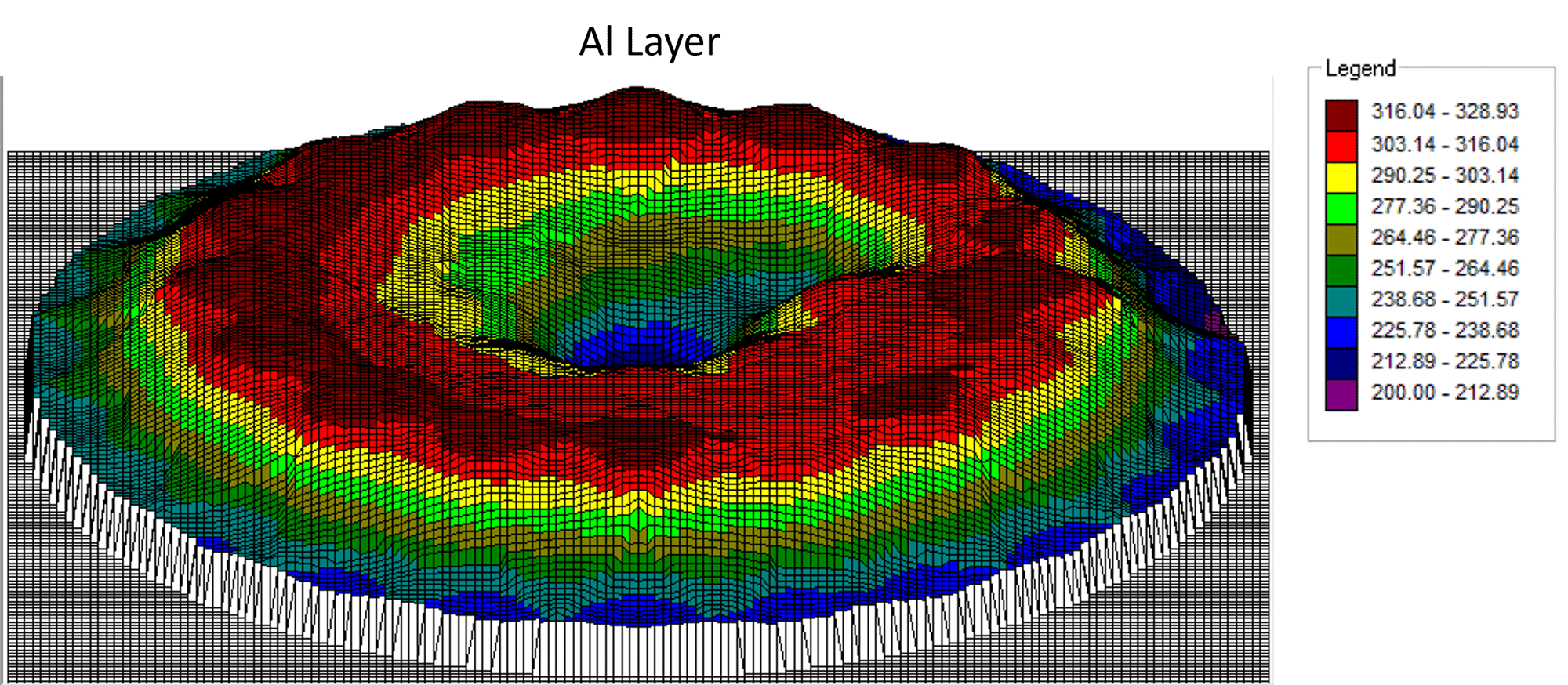
- 3D Scanner height measurement, area scan, wafer surface roughness, and bumps co-planarity
- Optimal configuration for bump inspection
- An array of 4 silicon drift detectors (SDD) with large active area and 123 eV FWHM (@5.9 keV) resolution
- Measures light (low-energy) elements (carbon, oxygen, magnesium, aluminum, and phosphorous) using an optional helium atmosphere and special SDD detectors
- Monochromatic or polychromatic x-ray options
- Inspects micro-features through focused vertical X-ray beam (down to 10 µm diameter for polychromatic optics and 20 µm diameter for monochromatic optics)
- Advanced motion platform for sub-micron accuracy
- Precise 3D geometrical inspection of features: micro-bumps, pillars, and pads
- Composition analysis associated with FinFET structures
- Fully automated calibration processes, ensuring long-term stability and consistency, and tube aging correction
- In line with SECS/GEM communication protocol
Combining advanced X-ray and optical techniques, the ONYX Series offers a unique wafer metrology approach in many areas, from FEOL through WLP, leading to in-line solutions for these processes. This sophisticated hybrid metrology tool enables high-throughput, in-line measurements on a blanket and product wafers ranging from ultra-thin single-layer films to multi-layer stacks.
The optical feature with 2D microscope and optional 3D scanner enables defect detection, sizing, and characterization of BEOL structures through image analysis (of critical dimensions, height, roughness, etc. of metal stacks, solder bumps, pillars, etc.) complemented by elemental composition and thickness measurements by ED-XRF analysis.
Hybrid configuration | automated x-ray analysis, 2D microscope, and optional 3D scanning for film stack, bumps, and composition measurements on blanket and patterned wafers
X-ray Optics Options
Polycapillary x-ray optics |
Monochromatic COLORS™-t x-ray optics |
| Provide polychromatic and enhanced performance of XRF analysis to identify a wide range of elements efficiently | Enables measurements in low background spectrum enabling effective analysis of low signals. • High brightness excitation • Small spots for a wide range of thin film applications. • Ideal configuration for bumps and copper pillars inspection |
Applications
THIN FILMS MEASURING AND MONITORING
Measure and monitor thickness and composition of precious metal thin films:
- Analyze ultra-thin films of any type of element, regardless of their physical properties
SINGLE-BUMP METROLOGY
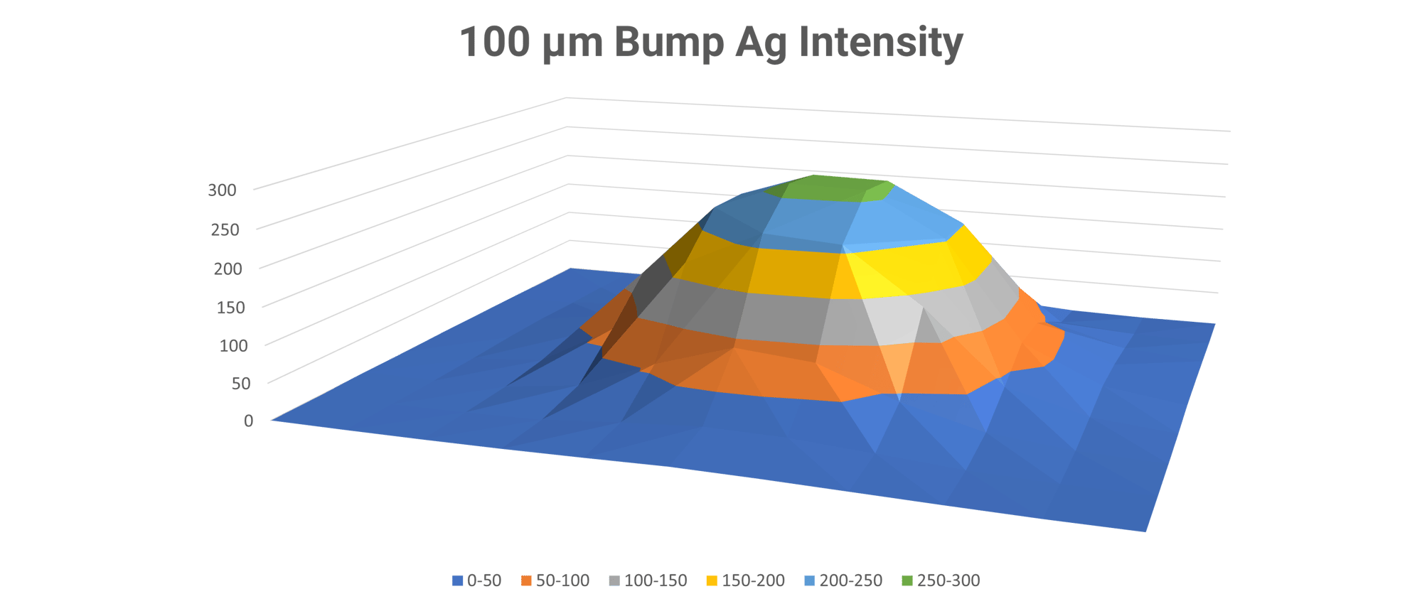
Measure and monitor Ag%, Sn%, Ni layers, Cu thickness, and total bump height:- Measure single-solder bumps as small as 10 μm diameter
- Inspect a range of parameters: across the wafer, wafer-to-wafer, and lot-to-lot
- Measure CD and a total height of single bumps using a 2D microscope, 3D scanner, and built-in sensors
UBM/RDL
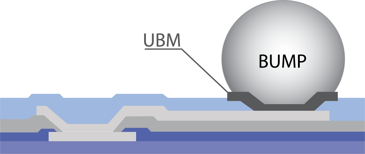
Conduct metallurgical inspections of under bump metallization (UBM) and redistribution layers (RDL):- Analyze multi-stack structures and thick monolayers, for layer thickness and composition
- Distinguish separate layers simultaneously
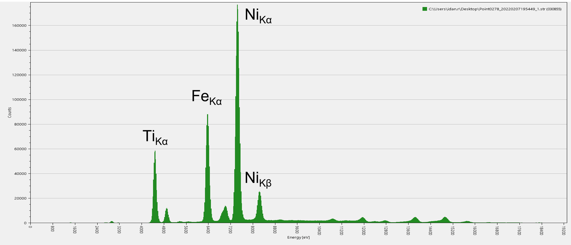
ALLOY COMPOSITIONS
Measure and monitor metals and alloy composition:
- Analyze metal elements (Ga, P, Co, Ni, Fe, Pt, Cr, Zn, and Mn)
- Identify alloys (NiFe, CoNi, NiP, NiPt, and CrMn)

Contact Us
Whether you are interested in getting a quote, want a demo, need technical support, or simply have a question, we're here to help.
