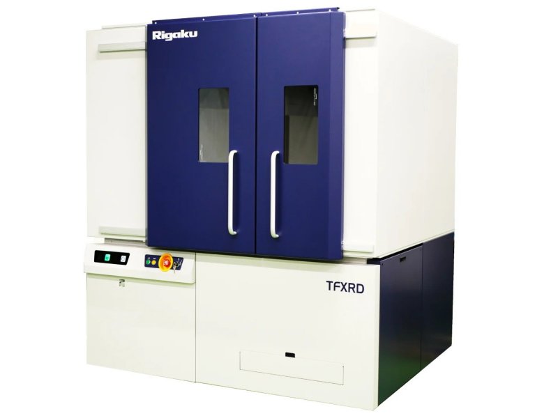
TFXRD Lab
High-precision thin film XRD for advanced research
The Rigaku TFXRD Lab delivers lab-grade precision for the non-destructive analysis of thin films, multilayers, and coatings. Designed for materials research laboratories working on thin films, multilayers, and coatings for next-generation electronic and photonic devices, this system features a high-precision goniometer with selectable optics and an XY-movable stage for mapping wafers up to 300 mm in diameter. With high-resolution measurements, flexible configuration, and exceptional sample integrity, the TFXRD Lab empowers scientists and engineers to accelerate materials discovery, optimize growth processes, and enhance device performance.
Available models:
- TFXRD Lab 200: Supports wafers up to 200 mm
- TFXRD Lab 300: Supports wafers up to 300 mm
TFXRD Lab Overview
High-precision goniometer with selectable optics
XRD System for all thin film XRD applications and XY movable stage for mapping up to 300 mm wafers.
The system guarantees that your samples will remain intact, ensuring you can conduct further experimentation and analysis without any issues. Trust us to provide the most precise and reliable results for all your research and development needs.
XRD system mapping tool for Near-fab applications
Improve materials analysis, enhanced quality control, and optimized manufacturing processes.
Thin films
- Precise thickness and composition
- Crystallographic information
- Stress and strain analysis
- Non-destructive characterization
- Multilayer analysis
- Advanced material development
Specialized for XRR thickness
Determine the thickness, density, and interface roughness of thin films, coatings, and multilayer structures.
GaAs (004), cubic GaN (002), hexagonal GaN (0004) specialized evaluation
Precise analysis of the crystallographic orientations and control the growth and processing of materials to achieve desired performance in electronic and optoelectronic devices.
TFXRD Lab Features
TFXRD Lab Specifications
| Technique | High-resolution thin film X-ray diffraction (HR-XRD) and X-ray reflectivity (XRR) | |
|---|---|---|
| Purpose | Non-destructive structural analysis of thin films, multilayers, and coatings for R&D applications | |
| Technology | High-precision θ-2θ goniometer with selectable optics and XY-movable stage for wafer mapping | |
| Key components | High-brilliance X-ray source; precision XRD optics; high-resolution 2D detector; enclosed cabinet | |
| Options | XRR module, automated mapping software, specialized analysis packages (GaAs, GaN, etc.) | |
| Wafer transfer / Sample handling | Manual wafer loading with XY stage (supports up to 300 mm wafers) | |
TFXRD Lab Events
Learn more about our products at these events
-
EventDatesLocationEvent website
-
The International Workshop on Gallium Oxide and Related Materials (IWGO-6)August 2 2026 - August 7 2026College Park, MD, USA.
-
SEMICON Taiwan 2026September 2 2026 - September 4 2026Taipei, Taiwan
-
ICSCRM Japan 2026 (Silver Sponsor)September 27 2026 - October 2 2026Yokohama, Japan
-
SEMICON West 2026October 13 2026 - October 15 2026San Francisco, CA, USA
-
SEMICON EuropaNovember 10 2026 - November 13 2026Munich, Germany
-
German Epitaxy WorkshopNovember 25 2026 - November 27 2026Freiburg, Germany
-
SEMICON Japan 2026December 9 2026 - December 11 2026Tokyo, Japan

Contact Us
Whether you are interested in getting a quote, want a demo, need technical support, or simply have a question, we're here to help.