
Accelerating Semiconductor Innovation Through Advanced X-ray Metrology
Meet Rigaku at booth N0592 at SEMICON Taiwan 2026: September 2-4, 2026
As AI drives the demand for advanced logic, HBM, and advanced packaging, semiconductor manufacturing is reaching new levels of complexity. Accurate, production-ready metrology is more critical than ever.
Join Rigaku at SEMICON Taiwan to discover how our X-ray metrology and inspection solutions help semiconductor manufacturers, foundries, OSATs, and materials suppliers accelerate innovation, improve yield, and gain deeper process insight across the entire semiconductor value chain.
View our Digital Metrology Solutions Guide.
Celebrate 75 years of innovation
Receive a complimentary Rigaku 75th Anniversary Journal
Schedule a meeting with Rigaku before the event and receive your complimentary anniversary journal during your booth visit (N0592, 4th floor, TaiNEX 1).
Available while supplies last.
Powering the future of semiconductor manufacturing
For 75 years, Rigaku has helped scientists, engineers, and manufacturers turn complexity into clarity.
Today, semiconductor leaders face new challenges:
- HBM process complexity
- Hybrid bonding integration
- Advanced packaging inspection
- Thin-film process control
- Next-generation memory architectures
- High-volume manufacturing scalability
Rigaku delivers advanced metrology solutions designed to provide actionable insights from R&D through high-volume production.
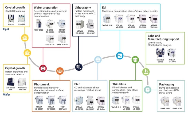
Rigaku across the semiconductor value chain
Comprehensive metrology solutions from crystal growth to advanced packaging
Whether optimizing next-generation logic devices, advanced memory products, or complex packaging architectures, Rigaku provides the measurement confidence needed for process success.

Featured technologies at SEMICON Taiwan
XTRAIA XD-3300
Direct analysis of superlattice structures on ultra-Small wafer pads
As semiconductor structures shrink and become increasingly complex, manufacturers require precise metrology on ever-smaller targets.
Ideal for advanced logic, memory, and emerging semiconductor technologies.
- High-resolution XRD/XRR measurements
- Superlattice characterization
- Measurements on ultra-small pads
- Faster process feedback
- Enhanced development productivity
XTRAIA MF-3400
Direct visualization of nanoscale structures
The XTRAIA MF-3400 provides non-destructive direct visualization and measurement of nanoscale semiconductor structures
- Simultaneous thickness and composition analysis
- Advanced multilayer characterization
- Improved process monitoring
- Reduced measurement times
- Increased manufacturing throughput
Advanced packaging solutions
ONYX Series
Non-destructive characterization of multilayer structures for:
- Advanced packaging
- HBM applications
- Hybrid bonding architectures
- BEOL process control
XHENA AX-3000
Advanced X-ray inspection technology supporting:
- Defect detection
- Failure analysis
- Process optimization
- Packaging quality control
Contact Us
Whether you are interested in getting a quote, want a demo, need technical support, or simply have a question, we're here to help.