
Non-destructive measurement with high sensitivity ensures contamination control at advanced nodes.

.jpg?width=800&name=XTRAIA%20MF-3400%20(1200%20x%20627).jpg)
XTRAIA MF-3400
Non-destructive thin film and multi-layer structure analysis.
Enables:
- • Film thickness measurement
- • Composition analysis
- • Multi-layer stack characterization
- • Process monitoring and control
.jpg?width=800&name=XTRAIA%20XD-3300%20(1200%20x%20627).jpg)
XTRAIA XD-3300
High-precision structural and compositional analysis for complex semiconductor architectures.
Ideal for:
- • Advanced device structures
- • Multi-layer thin films
- • Packaging materials
- • Emerging semiconductor materials
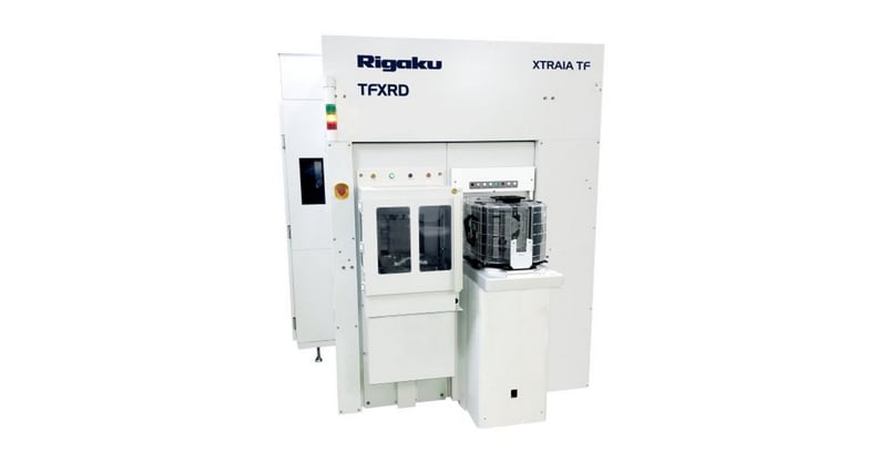
XTRAIA TF
Advanced X-ray thin-film metrology for precise structural and compositional characterization of semiconductor wafer stacks.
Ideal for:
- • Epitaxial and strained semiconductor layers
- • Complex multilayer thin films and gate stacks
- • Advanced logic and memory materials (SiGe, GaN, SiC, III-V)
- • Process monitoring for leading-edge device fabrication
In-line dual-head micro-spot XRF
ONYX 3200
EDXRF and optical hybrid metrology tool for automated X-ray analysis, 3D scanning, and 2D microscope for film thickness and composition measurements on blanket and patterned wafers for up to 300 mm wafers
- High-performance in-line dual-head micro-spot XRF
- Non-destructive wafer inspection and metrology
- Dual X-ray source (polycapillary / monochromatic)
- For up to 300 mm wafers.

XRTmicron Series
High-resolution X-ray topography for rapid crystal orientation and defect imaging of semiconductor wafers and substrates.
Ideal for:
- Crystal orientation mapping of wafers and ingots
- Defect and dislocation imaging in single-crystal substrates
- Quality control of SiC, GaN, and other advanced substrates
- Incoming wafer inspection for semiconductor manufacturing

Contact Us
Whether you are interested in getting a quote, want a demo, need technical support, or simply have a question, we're here to help.