
Bump Inspection - Composition & Height
The hybrid solution provides a quick and reliable location of bump and wafer defects. The bump, a dome-like structure made of solderable material, is a crucial interconnecting element for connecting chips in a three-dimensional stack and for connecting the stack to the printed circuit board.
- Elemental composition analysis by optical analysis for geometrical parameters and XRF
- Vertical incident X-ray beam (spot down to 7 µm on Sn K line) using four independent detectors configured in a symmetric assembly
- Thickness/composition extraction using robust Fundamental Parameters (FP) algorithm
- Composition analysis using Standardless Fundamental Parameter (SLFP) option

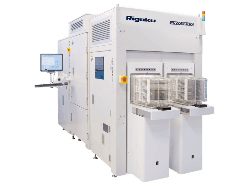
ONYX 3000
EDXRF and optical hybrid metrology tool for automated X-ray analysis, 3D scanning, and 2D microscope for film thickness and composition measurements on blanket and patterned wafers for up to 300 mm wafers
Learn more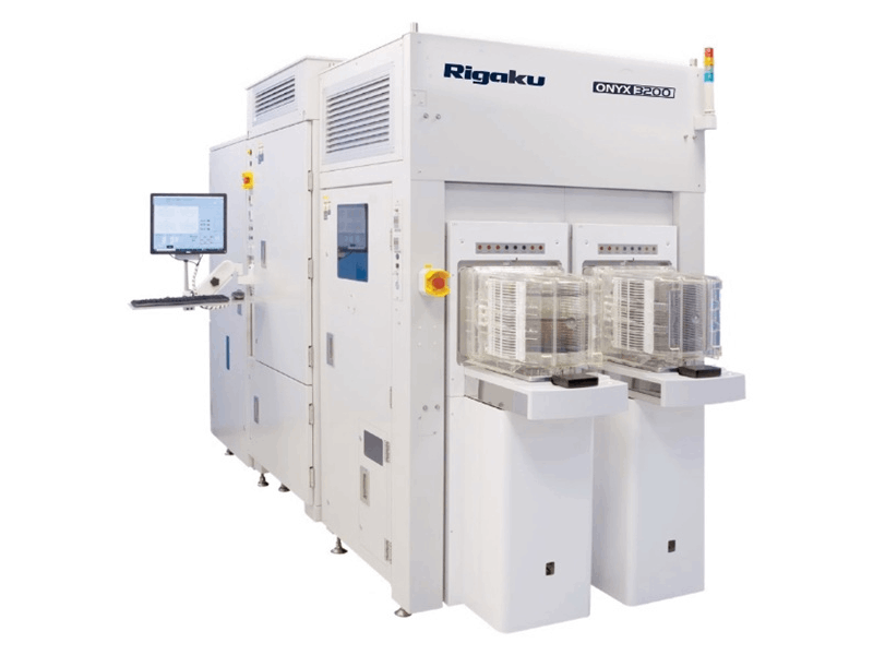
ONYX 3200
EDXRF and optical hybrid metrology tool for automated X-ray analysis, 3D scanning, and 2D microscope for film thickness and composition measurements on blanket and patterned wafers for up to 300 mm wafers
Learn more
Contact Us
Whether you are interested in getting a quote, want a demo, need technical support, or simply have a question, we're here to help.