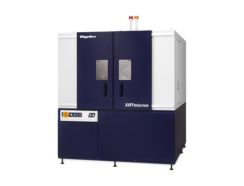
XRTmicron (Lab)
X-ray topography imaging system
For non-destructive evaluation of single-crystalline materials
Rigaku XRTmicron (Lab) is a fast, high-resolution laboratory X-ray topography system for non-destructive crystal defect imaging. Various types of dislocations, micropipes, stacking faults, small angle grain boundaries, and non-uniformity within single crystal wafers (such as Si, SiC, GaN, InP, GaAs, AlN, Ga₂O₃, sapphire, and more) can be imaged across wafers up to 300 mm in diameter.
XRTmicron (Lab) Overview
The XRTmicron (Lab) is designed for scientists conducting fundamental research in crystal growth and epitaxial layer formation. By providing high-resolution, non-destructive X-ray topography, it enables researchers to study the underlying physics of crystallographic defects and explore the mechanisms that govern material quality.
This system supports manual sample handling, from coupons to 300 mm wafers, with flexible configuration, aligns with the needs of laboratory environments, allowing scientists to design experiments, validate growth processes, and investigate defect formation at the earliest stages.
With the XRTmicron (Lab), researchers can push the boundaries of material science, gaining insights that not only advance academic knowledge and material discovery but also lay the groundwork for new applications in power electronics, optoelectronics, and beyond.
XRTmicron (Lab) Features
XRTmicron (Lab) Specifications
| Technique | X-ray topograph imaging | |
|---|---|---|
| Purpose | Non-destructive evaluation of single-crystalline materials | |
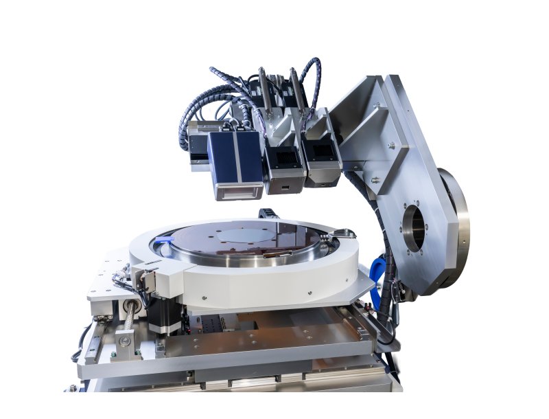
| Technology | Switch between transmission and reflection topography | |
| Key components | High-brightness micro X-ray source; specialized X-ray mirror optics; high-resolution, high-sensitivity X-ray camera | |
| Options | HR-XTOP camera, Crystal collimator, Defect inspection done with XRT Toolbox Software | |
| Wafer transfer / Sample handling | Manual handling | |
XRTmicron (Lab) Resources
Webinars
| Non-Destructive Dislocation Characterization in SiC Substrates Using XRTmicron Technology | Watch the Recording |
Rigaku Journal articles
| Read the Article | |
| Read the Article | |
| Read the Article | |
| Read the Article | |
| Read the Article |
Publications
XRTmicron (Lab) Events
Learn more about our products at these events
-
EventDatesLocationEvent website
-
The International Workshop on Gallium Oxide and Related Materials (IWGO-6)August 2 2026 - August 7 2026College Park, MD, USA.
-
SEMICON Taiwan 2026September 2 2026 - September 4 2026Taipei, Taiwan
-
ICSCRM Japan 2026 (Silver Sponsor)September 27 2026 - October 2 2026Yokohama, Japan
-
SEMICON West 2026October 13 2026 - October 15 2026San Francisco, CA, USA
-
SEMICON EuropaNovember 10 2026 - November 13 2026Munich, Germany
-
German Epitaxy WorkshopNovember 25 2026 - November 27 2026Freiburg, Germany
-
SEMICON Japan 2026December 9 2026 - December 11 2026Tokyo, Japan

Contact Us
Whether you are interested in getting a quote, want a demo, need technical support, or simply have a question, we're here to help.