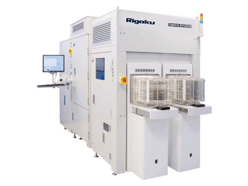
ONYX 3200
In-line Dual-head Micro-spot XRF
Non-destructive wafer inspection and metrology
Dual X-ray source (polycapillary / monochromatic)
For up to 300 mm wafers.
ONYX 3200 Overview
The ONYX 3200 is the most advanced hybrid metrology solution in the market; with its dual head, the second-generation tool combines advanced μXRF and optical techniques to provide high accuracy in defect detection and the highest throughput for in-line semiconductor manufacturing.
The ONYX series systems are designed to provide a holistic metrology approach in all steps of the manufacturing process from FEOL through WLP, including optimal configuration for advanced packaging and single bump applications to monitor Ag/Sn ratio—proven results in measuring and identifying single solder μ-bumps less than 5μm diameter.
Optimized source capability
- Single μ-bump measurements for process monitoring
- High yield and improved throughput
- Accurate analysis for metal thickness and composition
- Maximum sensitivity for layer thickness and composition
2D Microscope |
2D Microscope Magnification |
3D Scanner |
|
|
|
|


ONYX 3200 Features
ONYX 3200 Specifications
| Metrology type | Dual-head micro-spot EDXRF and optical inspection (2D-3D) | |
|---|---|---|
| Wafer size | Up to 300 mm | |
| Wafer type | Blanket and patterned wafers | |
| Navigation | Precise stage complemented with an image recognition algorithm Sub-micron fast navigation to single feature center |
|
| Micro XRF beam orientation | Vertical incidence micro-spot (µXRF) | |
| Optics | "Polychromatic” (X-ray optics) and COLORS “Monochromatic” (X-ray optics) | |
| Micro XRF beam spot size | 10-50 µm spot sizes adjustable | |
| Detector type | Silicon drift detector (SDD): 3 configurations 1. Regular > Al 2. Light-element: C, N, O, F, S 3. Heavy-element: > Ge (optimized for Ag, Sn) |
|
| DPP | Digital Pulse Processor | High efficiency of more than 1 million photons/sec. | |
| X/Y stage accuracy | 0.1 µm | |
ONYX 3200 Events
Learn more about our products at these events
-
EventDatesLocationEvent website
-
The International Workshop on Gallium Oxide and Related Materials (IWGO-6)August 2 2026 - August 7 2026College Park, MD, USA.
-
SEMICON Taiwan 2026September 2 2026 - September 4 2026Taipei, Taiwan
-
ICSCRM Japan 2026 (Silver Sponsor)September 27 2026 - October 2 2026Yokohama, Japan
-
SEMICON West 2026October 13 2026 - October 15 2026San Francisco, CA, USA
-
SEMICON EuropaNovember 10 2026 - November 13 2026Munich, Germany
-
German Epitaxy WorkshopNovember 25 2026 - November 27 2026Freiburg, Germany
-
SEMICON Japan 2026December 9 2026 - December 11 2026Tokyo, Japan

Contact Us
Whether you are interested in getting a quote, want a demo, need technical support, or simply have a question, we're here to help.