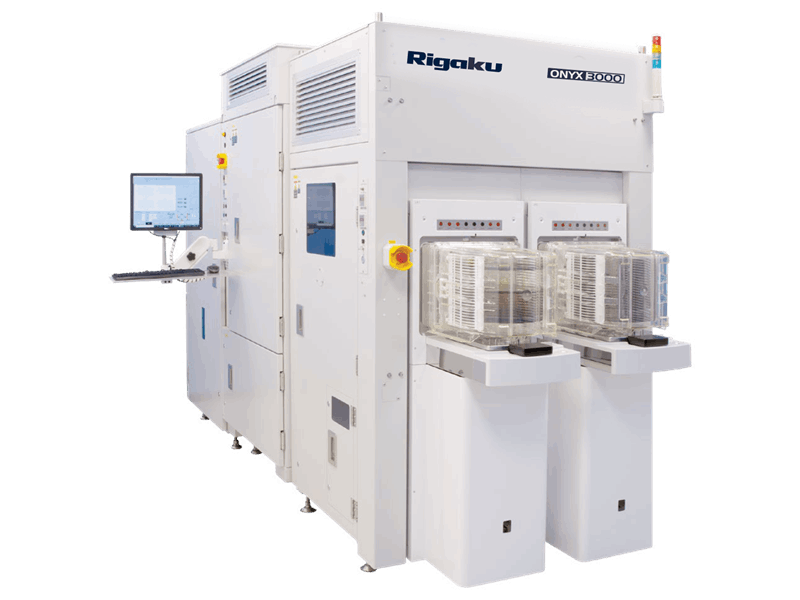
ONYX 3000
Micro-spot EDXRF and Optical Inspection (2D-3D)
In-line non-destructive inspection and metrology for the semiconductor and micro-electronics industries
Combining advanced X-ray and optical techniques, the ONYX 3000 offers a unique wafer metrology approach in many areas from FEOL through WLP, leading to in-line solutions for these processes. This sophisticated hybrid metrology tool enables high-throughput, in-line measurements on a blanket and product wafers ranging from ultra-thin single-layer films to multi-layer stacks.
ONYX 3000 Overview
The optical feature with 2D microscope and 3D scanner enables defect detection, sizing, and characterization of BEOL structures through image analysis (of critical dimensions, height, roughness, etc. of metal stacks, solder bumps, pillars, etc.) complemented by elemental composition and thickness measurements by EDXRF analysis.
Hybrid configuration | automated X-ray analysis, 3D scanning, and 2D microscope for film stack, bumps and composition measurements on blanket and patterned wafers
Layer-by-layer wafer inspection with qualitative and quantitative results
- XRF measures elemental composition and film thickness
- 2D Microscope used for pattern recognition, CD calculation.
- 3D Scanner height measurement, area scan, wafer surface roughness and bumps co-planarity
ONXY 3000 unique advantages
- Optimal configuration for bumps inspection
- Array of 4 silicon drift detectors (SDD) with large active area and 123 eV FWHM (@5.9 keV) resolution
- Measures light (low-energy) elements (carbon, oxygen, magnesium, aluminum, and phosphorous) using an optional helium atmosphere and special SDD detectors
- Monochromatic or polychromatic X-ray options
- Inspects micro-features through focused vertical X-ray beam (down to 10 µm diameter for polychromatic optics and 20 µm diameter for monochromatic optics)
- Advanced motion platform for sub-micron accuracy
- Precise 3D geometrical inspection of features: micro-bumps, pillars, and pads
- Composition analysis associated with FinFET structures
- Fully automated calibration processes, ensuring long-term stability and consistency, and tube aging correction
- In line with SECS/GEM communication protocols
X-ray optics options
Polycapillary X-ray optics |
Monochromatic COLORS-t X-ray optics |
| Provide polychromatic and enhanced performance of XRF analysis to identify a wide range of elements efficiently |
Enables measurements in low background spectrum enabling effective analysis of low signals.
|
ONYX 3000 Features
Hybrid configuration | automated x-ray analysis, 3D scanning, and 2D microscope for film thickness and composition measurements on blanket and patterned wafers.
2D Microscope |
2D Microscope Magnification |
3D Scanner |
|
|
|
|


ONYX 3000 Videos
ONYX 3000 Specifications
| System Parameters | Specifications | |
|---|---|---|
| Metrology type | Micro-spot EDXRF and optical inspection (2D-3D) | |
| Wafer size | Up to 300 mm | |
| Wafer type | Blanket and patterned wafers | |
| X/Y stage resolution | < 1 µm (Stage resolution 0.1 µm) | |
| Sample handling | Magazine robot | |
| Automation | Full wafer capability with single or dual automatic loader | |
| Navigation | Precise stage complemented with an image recognition algorithm. Sub-micron fast navigation to single feature center. |
|
| SW User Interface | Auto calibration. Ease-of-use recipe creation and maintenance. Fundamental parameters optional. | |
| Micro XRF beam orientation | Vertical incidence micro-spot µXRF | |
| X-ray tube energy | Up to 50 kV, 50 W | |
| Optics | Polycapillary / COLORS (monochromatic X-ray optics) |
|
| Micro XRF beam spot size | 10-50 µm spot sizes adjustable | |
| Detector type | Silicon drift detector (SDD) optional: light element detector (C,N,O,F.S) | |
| Detector resolution | 123 ± 5 eV with a large solid angle | |
| DPP | Digital Pulse Processor | High efficiency of more than 1 million photons/sec | |
ONYX 3000 Application Notes
The following application notes are relevant to this product
-
RSMD007 - Single Wafer Pass Detection & Metrology
-
RSMD004 - Pd Measurement on GaAs Wafer
-
RSMD-20104496 - Defect Sizing and Identification using 3D and XRF Review
-
RSMD-20101833 - Aluminum Oxide Film Thickness Measurement
-
RSMD-20220728 - Measurements of AgSn Micro Solder Bump using Monochromatic Micro X-ray Beam
-
RSMD-20101936 - Cu Seed Composition and Thickness
-
RSMD-20101835 - Ultrathin Film Thickness
-
RSMD-20101831 - Ultrathin Ru Thickness Measurement by Micro-spot EDXRF
ONYX 3000 Events
Learn more about our products at these events
-
EventDatesLocationEvent website
-
The International Workshop on Gallium Oxide and Related Materials (IWGO-6)August 2 2026 - August 7 2026College Park, MD, USA.
-
SEMICON Taiwan 2026September 2 2026 - September 4 2026Taipei, Taiwan
-
ICSCRM Japan 2026 (Silver Sponsor)September 27 2026 - October 2 2026Yokohama, Japan
-
SEMICON West 2026October 13 2026 - October 15 2026San Francisco, CA, USA
-
SEMICON EuropaNovember 10 2026 - November 13 2026Munich, Germany
-
German Epitaxy WorkshopNovember 25 2026 - November 27 2026Freiburg, Germany
-
SEMICON Japan 2026December 9 2026 - December 11 2026Tokyo, Japan

Contact Us
Whether you are interested in getting a quote, want a demo, need technical support, or simply have a question, we're here to help.