Application Note RSMD-20101936
PCB panel
Introduction
Seed copper is deposited during the PCB manufacturing process, often over other Cu layers, a process that requires accuracy in the thickness of this thin layer. Measurement of the seed layer thickness for quality assurance is available using Energy Dispersive X-ray Fluorescence (EDXRF), which overcomes the challenge of differentiating seed copper from the Cu layer beneath.
XRF Analysis
- XRF results of sample surface
- The following elements were detected: Cu, Al, Si, S, Fe, Ni, Cu
- Further analysis examples:
- Light element detection
- What other elements should be expected?
 Acquisition time: 30 sec
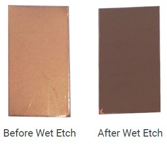
Wet etch
- Etch performed by dipping the sample (for one minute) in a solution containing:
- H₂0₂ (3%)
- Citric acid
- NaCl
Measurement objective
To measure the thickness of the top, electroless-deposited Cu seed layer at several sample locations.
Electroless Cu seeding (1 µm)

- ABF, Ajinmoto Build-up Film, is a carbon-based epoxy film developed by Ajinmoto Co.
- FR-4, flame retardant class 4, is a type of laminated substrate material used in the manufacture of printed circuit boards (PCBs).
Top Cu layer isolation
- The top Cu layer was removed from one of the samples using wet etch.
- XRF comparison was made between etch and non-etch samples.
- Cu Lα comes only from the top Cu layer.

Cu Lα saturation test
- For the top Cu layer, 1 µm is much below the saturation depth.
- Saturation in XRF is a specific depth of the layer whereby intensity no longer changes beyond this layer thickness.
- Thickness changes correlate to changes in the current.
- XRF measurement was performed at the same location using varying currents in order to determine the ideal linear section of the intensity vs. current curve.
Cu thickness sample comparison
- XRF scan was performed over six points (1 mm step) on three different samples.
- Cu Lα peak intensity was compared.
- The average intensity of Samples B and C were used as reference with thickness of 1 µm.
- Sample A has significantly thinner top Cu layer than Samples B and C.
- The top Cu layer of Samples B and C has uniform thickness, unlike Sample A.
Cu intensity

Intensity vs. current

Across-wafer variation

Cu layer thickness [µm]
| Point | Sample A | Sample B | Sample C |
| 1 | 0.42 | 1.00 | 1.00 |
| 2 | 0.52 | 1.01 | 1.01 |
| 3 | 0.64 | 1.01 | 1.01 |
| 4 | 0.65 | 1.01 | 0.98 |
| 5 | 0.74 | 0.97 | 1.01 |
| 6 | 0.78 | 0.99 | 0.99 |
| Average | 0.62 | 1.00 | 1.00 |
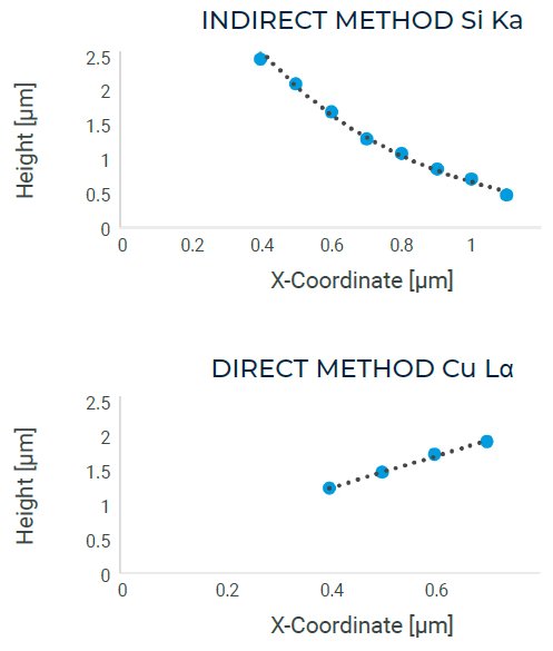
Cu seed thickness measurement by direct and indirect methods
- Cu layer thickness is measured by an automated algorithm using two methods.
- Direct method (0–0.7 µm) measuring the Cu Lα peak and calculating Cu layer thickness using linear regression
- Indirect method (0.7–1.4 µm) measuring the Si Kα peak and calculating Cu layer thickness using exponential regression
- Cu Lα peak intensity is saturated due to its low energy (0.93 keV), so the Cu layer thickness is measured indirectly using the Si from the ABF layer.

- Cu Lα and Si Lα were clearly detected by the EDXRF.
- Cu upper layer thickness can be monitored by using both peaks independently – Cu Lα or Si Kα peaks.
- Acquisition time: 12 sec
| Nominal [µm] | Direct Method [µm] | Indirect Method [µm] |
| 0.4 | 0.398 | 0.382 |
| 0.5 | 0.496 | 0.462 |
| 0.6 | 0.613 | 0.571 |
| 0.7 | 0.689 | 0.704 |
| 0.8 | - | 0.788 |
| 0.9 | - | 0.888 |
| 1.0 | - | 0.960 |
| 1.1 | - | 1.083 |
Regression curves
- Linear regression for the direct method
- Exponential regression for the indirect method
Roughness
- 3D scanner was used for measuring roughness by measuring surface height variations.
- Height variation up to 2 µm
3D scan imaging

2D microscope image

 Summary
- XRF is very sensitive to thickness variation up to 0.1 nm. Many elements can be analyzed, qualitatively and quantitatively.
- Top Cu layer thickness can be measured using Cu Lα peak intensity changes.
- For accurate results, standards are required.
- The 3D scanner can monitor surface roughness.
