XRD for Electronic Devices
X-ray diffraction (XRD), high-resolution X-ray diffraction (HRXRD), X-ray reflectivity (XRR), and small-angle X-ray scattering (SAXS) help electronic device developers and manufacturers connect crystal structure, film quality, nanoscale architecture, and process control to device performance. In semiconductors, displays, sensors, memory devices, power electronics, photovoltaic materials, and advanced packaging, performance depends on more than chemistry alone. Strain, crystallographic orientation, epitaxy, phase purity, thickness, density, roughness, interface quality, residual stress, and nanoscale ordering can all affect yield, reliability, speed, efficiency, and lifetime.
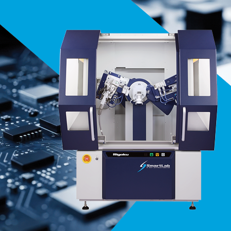
Rigaku X-ray diffraction, scattering, and semiconductor metrology solutions support electronic device workflows from R&D and materials development to process optimization, failure analysis, and production control. SmartLab and SmartLab SE are especially relevant for multipurpose XRD, thin film diffraction, SAXS, non-ambient work, pole figure, residual stress, and advanced method development. Rigaku’s semiconductor metrology portfolio also includes HRXRD systems for high-resolution, high-throughput measurements on blank and patterned wafers, including strain, thickness, composition, and crystalline quality analysis.
Connecting crystal structure, thin film quality, and device performance
Electronic devices depend on materials that are often thin, layered, strained, textured, nanoscale, or highly engineered. XRD-based methods provide non-destructive structural information that helps evaluate how deposition, annealing, etching, doping, lithography, packaging, and thermal cycling affect device materials and manufacturing consistency.
- Semiconductor crystal quality: Use HRXRD and rocking curve analysis to evaluate epitaxial layers, compound semiconductors, silicon-based structures, wide-bandgap materials, and other crystalline device materials. These measurements help assess crystalline quality, mosaicity, defects, strain, and process-driven variation.
- Strain, composition, and thickness analysis: Use HRXRD and reciprocal space mapping to characterize strained layers, superlattices, heterostructures, and epitaxial films. These analyses are important for advanced semiconductor devices where lattice mismatch, composition, and layer thickness directly affect electrical and optical performance.
- Thin film phase identification: Use XRD and grazing incidence XRD to identify crystalline phases in deposited films, transparent conductive oxides, dielectrics, ferroelectrics, piezoelectrics, magnetic films, phase-change materials, battery-device layers, and photovoltaic absorbers.
- X-ray reflectivity: Use XRR to measure film thickness, density, roughness, and interface quality in single-layer and multilayer stacks. This supports process development and QC for coatings, barriers, dielectrics, metal films, multilayers, and nanoscale device structures.
- Texture and preferred orientation: Use pole figure and texture analysis to evaluate crystallographic orientation in thin films, wafers, foils, electrodes, magnetic layers, interconnects, and packaging materials. Orientation can strongly influence conductivity, piezoelectric response, optical behavior, adhesion, and mechanical reliability.
- Residual stress analysis: Measure stress in films, coatings, metallization layers, wafers, MEMS structures, solder joints, and packaged components. Residual stress data can help explain cracking, delamination, warpage, fatigue, and reliability failures.
- SAXS and nanoscale structure: Use SAXS or grazing incidence SAXS to characterize nanoscale periodicity, pores, domains, nanoparticles, line/space structures, self-assembled materials, and other nanoscale features used in advanced electronic materials. SAXS is especially useful when nanoscale morphology affects optical, electrical, dielectric, or mechanical behavior.
- Photovoltaic and display materials: Analyze crystalline phases, texture, thin film quality, and multilayer structure in photovoltaic absorbers, transparent conductors, OLED-related films, quantum dot materials, oxide electronics, and display coatings.
- Packaging and reliability: Characterize solders, intermetallic compounds, underfills, ceramic substrates, thermal interface materials, metal coatings, and corrosion or oxidation products. XRD supports root-cause analysis when devices fail due to thermal cycling, humidity exposure, mechanical stress, or process variation.
- Process development and production control: Use XRD-based metrology to compare wafers, lots, deposition recipes, annealing conditions, and supplier materials. Non-destructive measurements support faster feedback loops, tighter process windows, and improved device consistency.
For advanced electronic device research and thin film characterization, SmartLab and SmartLab SE provide flexible XRD and scattering capabilities, including powder diffraction, thin film diffraction, SAXS, in-plane scattering, pole figure, residual stress, non-ambient measurements, and method development. For semiconductor manufacturing and wafer-level metrology, Rigaku HRXRD systems support high-resolution, high-throughput analysis of strain, thickness, composition, and crystalline quality on blank and patterned wafers. For routine materials verification, powders, ceramics, solders, and supporting components used in electronics manufacturing, MiniFlex and MiniFlex XpC provide compact XRD options for phase identification, phase quantification, crystallite size and strain, lattice parameter refinement, and Rietveld analysis.
Recommended products
Subscribe to the Bridge newsletter
Stay up to date with materials analysis news and upcoming conferences, webinars and podcasts, as well as learning new analytical techniques and applications.
Contact Us
Whether you're interested in getting a quote, want a demo, need technical support, or simply have a question, we're here to help.