
CT Lab HR160
High-resolution X-ray CT made simple
160 kV. Submicron details. One simple CT system.
The Rigaku CT Lab HR160 provides a simpler path to 160 kV submicron CT (computed tomography) for research, process development, and design engineering. Reveal internal structures with true 250 nm spatial resolution and a minimum voxel size of 62 nm—without complex workflows or hardware reconfiguration.
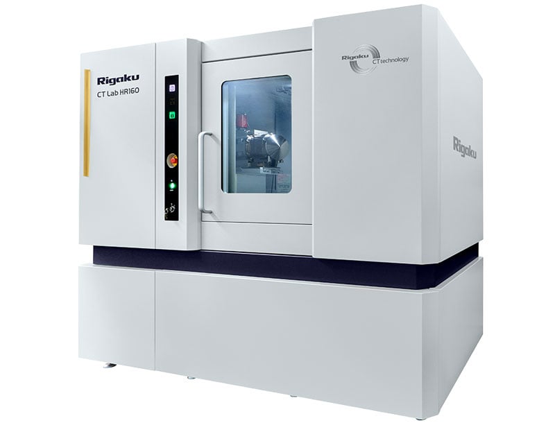
CT Lab HR160 Overview
Uncompromising high-resolution CT, now within reach for every lab
High-end CT scanners often include specialized measurement techniques and complex configurations that increase both cost and operational complexity. CT Lab HR160 focuses on the capabilities that matter most for practical research and engineering: 160 kV X-ray versatility, true 250 nm spatial resolution, a 62 nm minimum voxel size, and a straightforward workflow.
Its lens-free cone-beam geometry allows the field of view and resolution to be adjusted simply by changing the source-to-object distance and source-to-detector distance. No source, detector, or lens changes are required. This streamlined architecture makes it easier to move between samples and imaging requirements while minimizing setup time and hardware reconfiguration.
See both the big picture and the fine details
CT Lab HR160 combines a flexible field of view with true submicron imaging. The field of view ranges from 0.18 mm in diameter × 0.14 mm tall to 103 mm in diameter × 81 mm tall per scan. This flexibility allows users to inspect larger structures and then focus on small regions of interest for detailed analysis.
For example, an entire RAM stick can be scanned before zooming in to investigate micron-scale solder-joint defects, wire connections, buried circuits, connectors, and integrated-circuit layer integrity. Because the sample remains intact, internal structures can be studied without physical cross-sectioning.
One streamlined CT workflow
CT imaging requires scan-condition optimization, projection-image collection, reconstruction, and review of the resulting 3D volume. CT Lab HR160 simplifies this process with a one-flow-bar software interface that guides users through scan configuration and acquisition.
Reconstruction can be performed automatically, and reconstructed volumes can be loaded directly into CT Viewer for immediate review. The simplified workflow reduces trial and error, helps new users become productive more quickly, and lets experienced users move faster from sample setup to results.
Broad materials and application versatility
The combination of 40–160 kV operation, a 16.6 W nanofocus transmission X-ray source, flexible cone-beam geometry, and submicron imaging supports samples ranging from organic materials to electronic components.
Batteries
Visualize pores, cracks, and material inhomogeneity within and between battery electrode particles. Three-dimensional imaging can distinguish interparticle and intraparticle defects and help researchers investigate how manufacturing quality and cycling-induced degradation affect mechanical stability, capacity retention, reliability, and battery lifetime.
Electronics
Inspect printed circuit boards and small electronic components non-destructively. CT Lab HR160 can reveal solder-joint voids, broken or thinning connections, electrode layers, cracks, buried circuits, and dimensional variations while preserving the device for further testing.
Submicron imaging also supports detailed examination of multilayer ceramic capacitors and inductors, including electrode thickness and spacing, void distribution, thinning, and discontinuities that may affect electrical performance and reliability.
Advanced materials
Reveal voids, cracks, porosity, fiber orientation, delamination, adhesive bonds, weak interfaces, and other internal features in composites, resins, polymers, and molded materials. Non-destructive three-dimensional inspection helps connect processing conditions and microstructure with strength, reliability, damage, and long-term performance.
Additive manufacturing
Visualize and quantify cracks and pores in additively manufactured parts, including micropores within feedstock powders. The resulting data can help distinguish defects introduced during fabrication from those inherited from the feedstock and support process optimization, quality assurance, and failure analysis.
Medical devices and pharmaceuticals
Study the internal structure, function, and failure mechanisms of devices such as stents and implants without destroying the sample. Submicron X-ray CT can also reveal coatings, pores, internal defects, and other fine structures in pharmaceutical tablets and particles.
CT Lab HR160 Features
CT Lab HR160 Specifications
| Minimum voxel size | 62 nm | |
|---|---|---|
| Maximum field of view (FOV) | 103 mm diameter × 81 mm tall per scan | |
| Source-to-object distance (SOD) | 1.0 – 584 mm | |
| Source-to-detector distance(SDD) | 200 – 800 mm | |
| Maximum sample/object size | φ250 mm × H450 mm (XYZ = 0; no travel) φ200 mm × H200 mm (full XYZ travel) |
|
| Sample rotation | -180 - 540º | |
| Best spatial resolution | 250 nm @ 300 nm focus size | |
| Maximum sample/object weight | 10 kg | |
| Scan modes | Standard, stitched, half | |
| Geometry | Lens-free cone-beam geometry | |
| X-ray source | Maximum 16.6 W | |
| X-ray energy | W anode, adjustable applied voltage 40-160 kV | |
| Detector | High-resolution CMOS | |
| Detector pixel size | 49.5 × 49.5 μm | |
| Detector size | 2352 × 2944 pixels | |
| Detector active area | 116.4 mm × 145.7 mm | |
| Dimensions | 2040 (W) x 990 (D) x 1825 (H) mm | |
| Weight | 1850 kg (including the CT system, X-ray generator unit, and radiation shield) | |
CT Lab HR160 Resources
CT Lab HR160 Events
Learn more about our products at these events
-
EventDatesLocationEvent website
-
Battery Show 2026October 12 2026 - October 15 2026Detroit, MI, USA
-
Gulf Coast Conference (GCC) 2026October 13 2026 - October 15 2026Galveston, TX, USA
-
AAPS PharmSci 360 - 2026October 25 2026 - October 28 2026New Orleans, LA, USA
-
MATERIAUX 2026November 16 2026 - November 20 2026Grenoble, France
-
Advanced Automotive Battery Conf 2026December 8 2026 - December 11 2026Las Vegas, NV, USA
Contact Us
Whether you're interested in getting a quote, want a demo, need technical support, or simply have a question, we're here to help.