Micro-area Mapping Measurement of Printed Circuit Boards
Introduction
When analyzing a sample consisting of an extremely large number of micro-size parts, such as PCBs (printed circuit boards), it is necessary for the evaluation of the crystalline state of each part to use a focused X-ray beam and irradiate only a specific part. Optical systems in the past employed slits and collimators to convert the divergent beam emitted from the X-ray focal spot to a point focus beam. The downside to this technique is the large attenuation of the X-ray beam intensity, requiring a long time for micro-area measurement to be completed. By using the SmartLab μHR, a SmartLab model with microfocus optics, in combination with a high-speed 2D X-ray detector, a high-intensity micro-area measurement is possible in a short time even though the XG output is 1/10 of those in the past.
Measurements and results
The SmartLab μHR is equipped with a microfocus rotating anode X-ray tube. The X-ray beam is monochromatized and converted to a parallel beam 1 mm × 1 mm in diameter by using CMF microfocus optics. The beam width is narrowed by a collimator. As a result, as indicated in Fig. 1 and Table 1, compared with a collimator and the CBO-f point focus optics used in the past, a high-resolution and high-brilliance measurement was achieved even though the XG output is less than 1/10.
Micro-area measurement of PCB was performed using the SmartLab μHR. In both measurement points, identification of compounds included in micro-area of PCB and the orientation of coarse particles can be confirmed in an extremely short amount of time of approx. two minutes.
Table 1: Intensity and FWHM of optics
| Optics | XG output (kW) | Beam size (mm) | Normalized intensity | Brilliance (Intensity / Beam size) |
| SmartLab μHR | 0.8 | 0.3φ | 52.10 | 579 |
| SmartLab CBO‑f | 9.0 | 0.5φ | 53.45 | 68.1 |
| SmartLab collimator | 9.0 | 0.3φ | 1.00 | 3.5 |
.jpg?width=550&height=391&name=B-XRD1089%20Figure%201%20Data%20comparison%20of%20optics%20(Sample%20Si).jpg) Figure 1: Data comparison of optics (Sample: Si)
Figure 1: Data comparison of optics (Sample: Si)
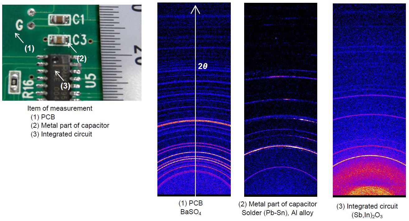 Figure 2: Micro-area measurement of PCB (Measurement time approx. two minutes)
Contact Us
Whether you're interested in getting a quote, want a demo, need technical support, or simply have a question, we're here to help.