Electronics
Rigaku's advanced analytical technology provides proven material analysis, identification, and quantitation, helping you create safe, efficient, and trustworthy electronic devices.
Wafer fabrication
Before growing the film, evaluate grains and crystal defects in the mono-crystal substrate for optimum device performance.
Learn more >
Film growth, electrode deposition
Our high-resolution and high-speed X-ray diffraction systems are capable of independently determining the critical parameters of crystalline perfection and thickness of thin-film layers which directly impact device performance with high-precision.
Learn more >
Dicing and packaging
To measure the individual components of a chip, an instrument capable of analyzing small regions of a semiconductor device is needed. By employing an X-ray diffraction system with micro-focus optics, along with a high-speed 2D detector, quick and accurate measurements of micro-areas with high intensity can be carried out.
Learn more >
Printed circuit boards (PCBs)
X-ray imaging is an essential method to non-destructively visualize the inner structure and defects of a single chip on a PCB by using 3D volume reconstruction and 2D slice rendering.
Learn more >.png?width=800&name=Principle%20of%20X-ray%20Topography%20(Transmission).png)
Crystal defects
When producing high-performance semiconductor devices, crystalline defects in epitaxial thin films can cause problems. For instance, when thin films are grown epitaxially, they may inherit crystal defects from the single crystal substrate. Therefore, it is crucial to assess the grains and crystal defects within the single crystal substrate before film growth to ensure optimal device performance.
Learn more >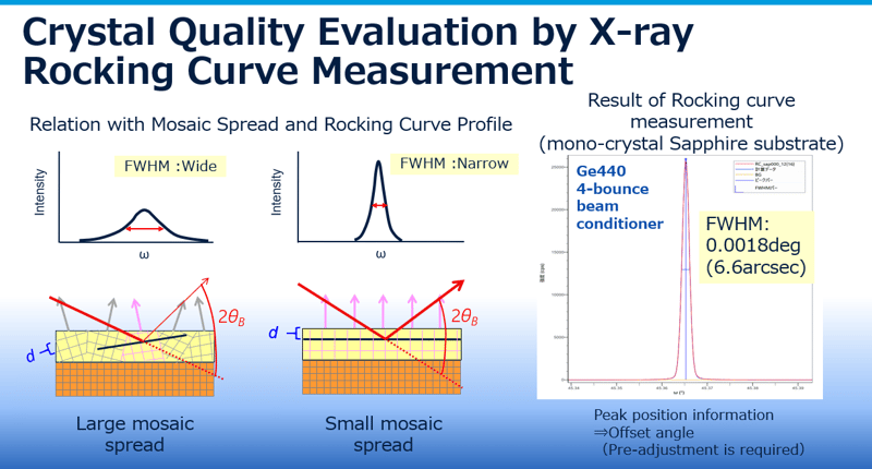
Crystal quality
X-ray rocking curve measurement is a method used to evaluate the crystal quality of both crystalline films and mono-crystal substrates. The width of the peak (FWHM) of the measured rocking curve profiles provides information about the orientation distribution of crystal lattice planes (mosaic spread) within the sample. This orientation distribution can be used as a measure of the sample's perfection. Rigaku’s SmartLab diffractometer, with its high-resolution beam conditioner, provides the necessary resolution to determine the perfection of high-quality crystalline films and substrates.
Learn more >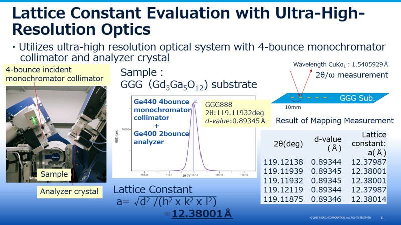
Lattice constants
Triple-axis X-ray geometry combined with a highly accurate goniometer can enable ultra-high resolution diffraction analysis of single-crystalline substrate wafers. The term "triple axis" refers to three independent crystalline diffraction components. The sample forms one axis, while the other two axes are associated with the incident and diffracted beam channel-cut multi-bounce monochromator crystals. By using an XY mapping stage, the variability of the crystalline lattice parameter can be evaluated across a single-crystal wafer.
Learn more >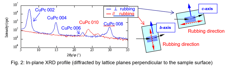
Orientation analysis
Organic semiconductors are a highly promising class of materials for the next generation of semiconductors. They are cost-effective and exhibit superior characteristics compared to conventional inorganic materials. The arrangement and orientation of molecules are critical to the properties of organic semiconductors. In this example, we highlight the benefits of using in-plane X-ray diffraction (XRD) to evaluate the orientation of a copper phthalocyanine (CuPc) thin film. This material is photoconductive and electroluminescent, making it a valuable organic material for various applications.
Learn more >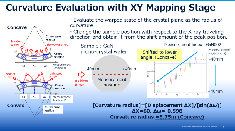
Curvature
Differences in thermal expansion between epitaxial films and their associated single-crystal substrates can cause the samples to warp. The extent of the induced curvature can be evaluated by analyzing X-ray rocking curve mapping data that is collected using an XY translation stage. Understanding the degree of curvature can serve as an indicator of residual stress within the film.
Learn more >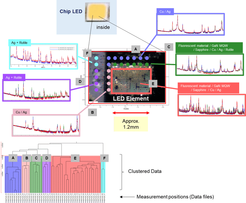
Dicing and packaging
The SmartLab μHR is an advanced system that can analyze the crystalline state of micro-parts like printed circuit boards. It uses a micro-focus X-ray source and high-speed 2D X-ray detector to perform high contrast micro-area measurements in a shorter amount of time compared to earlier systems that employed X-ray optics consisting of slits and collimators.
Learn more >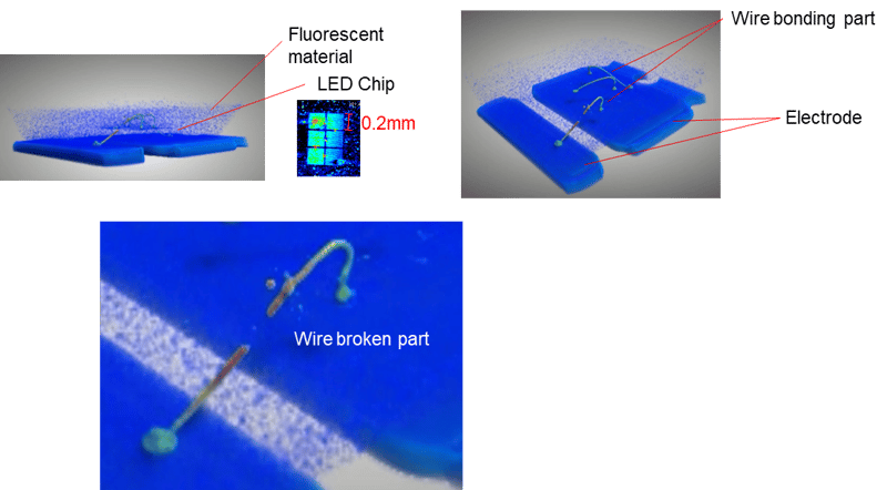
Printed circuit boards
X-ray micro CT (Computed Tomography) is a technique used to produce a high-resolution 3D image of a very small object. This is done by reconstructing projection images of X-rays that are transmitted through the object. The reconstructed image can be displayed in 2D cross-sections (slices) and 3D volume renderings, allowing for non-destructive analysis of the object's inner structure and defects.
Learn more >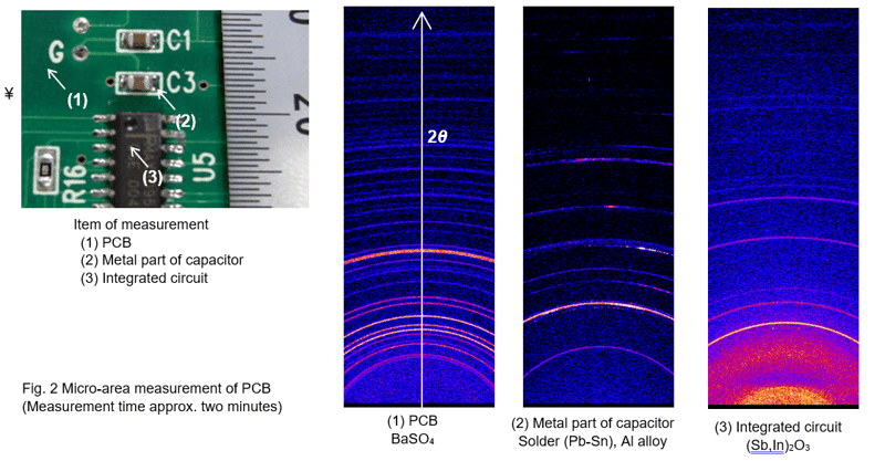
Micro-area mapping
To analyze micro-size parts such as PCBs, it's crucial to evaluate the crystalline state of each part. Traditional optical systems needed to convert divergent X-ray beams into a focused beam, which took a long time due to the large attenuation of the X-ray beam intensity. However, with the SmartLab μHR and a high-speed 2D X-ray detector, it's possible to achieve a high-intensity micro-area measurement in a short time, even with 1/10 of the X-ray generator output.
Learn more >
Contact Us
Whether you are interested in getting a quote, want a demo, need technical support, or simply have a question, we're here to help.