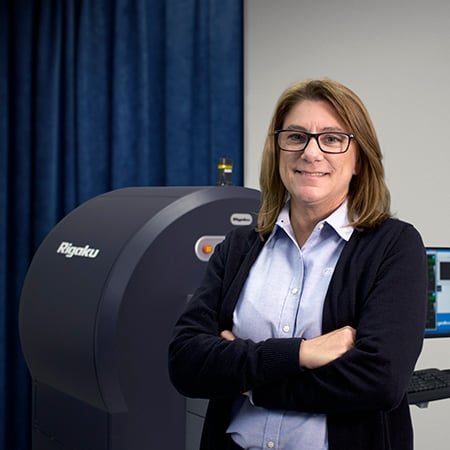
High-voltage micro-CT system CT Lab HV
Ted Huang and Angela Criswell
Winter 2025 Volume 41, No. 1 , 28-33
The CT Lab HV, developed by Rigaku, features a 225 kV X-ray source, a high-precision rotation stage, and a large detection area, enabling a broad variety of high-resolution imaging applications. Application examples, including additively manufactured superalloys and lithium-ion battery protection boards, highlight its effectiveness in defect detection, structural analysis, and product simulation. As demand for advanced imaging grows, the CT Lab HV offers an innovative solution for industry and research, enhancing the adoption of X-ray CT in critical applications.
Highlights
- High-voltage micro-CT extends nondestructive 3D imaging to dense, high-mass samples such as metal additive-manufactured parts, battery assemblies, and electronic components by using X-ray energies up to 225 kV.
- A combination of high penetration power, a large-area detector, flexible magnification, and a high-capacity sample stage enables imaging from micrometer-scale internal features to objects as large as 600 mm in diameter, 1200 mm tall, and 50 kg.
- CT data can support more than defect detection: reconstructed volumes can be segmented, dimensionally analyzed, quantified for void content, and converted into models for mechanical simulations based on the actual manufactured structure.
Summary
X-ray computed tomography provides nondestructive three-dimensional visualization of internal structures, allowing dense or complex objects to be examined without sectioning or extensive sample preparation. Unlike optical microscopy or SEM, which primarily examine exposed surfaces or prepared cross-sections, CT reconstructs the full internal volume and can identify pores, cracks, voids, delamination, misalignment, leakage, and other structural abnormalities.
For absorption-based CT, penetration and contrast depend strongly on sample thickness, density, elemental composition, and X-ray photon energy. Dense, thick materials containing relatively high-atomic-number elements absorb X-rays more strongly and therefore require higher-energy radiation to obtain usable transmitted intensity. This becomes particularly important for emerging applications involving lithium-ion battery assemblies, electronic circuitry, and metal additive manufacturing, where high-density materials and substantial sample dimensions are common.
A high-voltage micro-CT configuration using a 225 kV, 300 W X-ray source addresses these requirements. The system combines a minimum X-ray source focus size of 3 µm with a 434 × 434 mm flat-panel detector, variable source-to-object and source-to-detector distances, and a high-precision direct-drive rotation stage. It provides fields of view from approximately 4 to 350 mm, a minimum voxel size of 1.5 µm, and demonstrated spatial resolution of 3 µm. The large sample chamber also permits automated sample handling and customized experimental configurations.
Higher tube voltage is especially important for suppressing beam-hardening artifacts in dense materials. Comparison of high- and lower-voltage scans of an Inconel superalloy structure showed that 225 kV operation produced clearer internal contrast and substantially reduced artifacts compared with 130 kV imaging. In some applications, similar signal-to-noise performance can also be obtained at shorter exposure times.
For an additively manufactured Inconel structure, 200 kV imaging generated sufficient grayscale contrast to segment the solid material through relatively simple thresholding. The reconstructed volume was subsequently used to map structural thickness throughout the internal lattice. The same CT-derived geometry could be converted into a surface mesh and subjected to mechanical load simulation, demonstrating how CT can connect the actual manufactured component with a virtual engineering model rather than relying exclusively on its nominal CAD geometry.
High-voltage CT is also applicable to battery and electronics inspection. Imaging of a lithium-ion battery protection board resolved MOSFET wiring and connections approximately 40 µm and 125 µm in dimension, as well as features such as a solder layer of roughly 21 µm and a board layer of about 32 µm. Three-dimensional segmentation of solder joints allowed internal voids to be located and their volumes quantified from voxel counts. This illustrates how CT can provide both qualitative visualization and quantitative defect analysis in assembled battery components without physically dismantling them.

Frequently asked questions
-
Dense and thick materials absorb a large fraction of incident X-rays, particularly when they contain higher-atomic-number elements. Increasing the X-ray photon energy improves penetration and provides more transmitted intensity at the detector. A system operating at up to 225 kV can therefore image samples that are difficult to examine effectively with lower-voltage micro-CT. Higher voltage also reduces severe beam-hardening artifacts and can produce more clearly defined internal structures in dense metal parts and assembled products.
-
X-ray attenuation depends on the material's thickness, density, elemental composition, and the photon energy of the incident beam. Increasing thickness, density, or average atomic number generally increases absorption. Raising the photon energy reduces absorption sufficiently for more radiation to pass through a dense sample and reach the detector. Selecting an appropriate energy therefore involves balancing penetration with the contrast needed to distinguish internal structures.
-
The described high-voltage configuration can accommodate samples up to approximately 600 mm in diameter, 1200 mm in height, and 50 kg in mass. Its adjustable imaging geometry provides fields of view from about 4 to 350 mm and a minimum voxel size of 1.5 µm. With a minimum X-ray source focus size of 3 µm, spatial resolution of approximately 3 µm was demonstrated using a resolution phantom. This broad range allows both relatively large assemblies and fine internal details to be investigated with the same platform.
-
Metal additive-manufactured components can contain substantial thicknesses of dense alloys that preferentially absorb lower-energy X-rays from the incident spectrum. As the beam passes through the sample, its energy distribution changes, creating beam-hardening artifacts that can distort grayscale values and obscure internal structures. Higher tube voltage provides more penetrating radiation, reducing these artifacts and producing more consistent contrast for segmentation, defect detection, and dimensional analysis.
-
The reconstructed CT volume represents the actual manufactured geometry, including internal lattice structures and deviations that may not be represented accurately by the original design model. The solid structure can be segmented from the CT data and converted into a surface mesh. That mesh can then be imported into simulation software for calculations such as mechanical loading and stress analysis. This approach connects nondestructive inspection directly with simulation of the physical component as manufactured.
-
Yes. After reconstructing the protection-board volume, individual solder regions can be segmented and internal voids identified. Because each reconstructed voxel represents a known volume, the total volume of individual solder voids can be calculated from the number of voxels they occupy. The resulting defects can then be classified or color-coded by volume, providing a quantitative assessment of solder-joint quality in addition to visual inspection.
-
High-resolution CT can reveal wiring, wire connections, solder layers, circuit-board structures, MOSFET components, capacitors, and internal solder voids without dismantling the battery assembly. In the demonstrated measurements, wiring and connections of approximately 40 µm and 125 µm were visible, while a solder layer of about 21 µm and a board layer around 32 µm could also be measured. This makes the technique useful for examining connectivity, joint integrity, and manufacturing defects in compact electronic assemblies.
-
Optical microscopy and SEM provide very detailed surface or cross-sectional information, but they generally require access to the region being examined and may involve destructive sectioning or sample preparation. Micro-CT instead provides a complete three-dimensional view of internal structures nondestructively. It can therefore be used to locate defects, identify regions of interest, measure internal geometry, and guide subsequent microscopy or other analytical work while preserving the original sample.
Subscribe to the Bridge newsletter
Stay up to date with materials analysis news and upcoming conferences, webinars and podcasts, as well as learning new analytical techniques and applications.
Contact Us
Whether you're interested in getting a quote, want a demo, need technical support, or simply have a question, we're here to help.