
When nanometers decide everything
Advancing nanoelectronics requires measurement technologies that go beyond surface inspection. Increasingly complex materials, three-dimensional architectures, and heterogeneous integration demand non-destructive insight into structure, composition, strain, and interfaces.
At FCMN, the global community comes together to advance characterization methods that enable deeper understanding and more confident process decisions. Rigaku brings decades of X-ray innovation experience to this evolving measurement landscape.
Lab to Fab strategy
Rigaku’s Lab to Fab strategy ensures continuity between early-stage research and production environments. By combining advanced X-ray diffraction, fluorescence, scattering, and imaging techniques, Rigaku supports measurement workflows that scale with device complexity.
Key capabilities include:
- Thin film thickness, density, and composition analysis
- Crystal structure, strain, and defect characterization
- Interface and buried layer analysis
- Surface contamination detection
- Patterned feature and dimensional metrology
X-ray core expertise
Rigaku develops X-ray sources, optics, detectors, and analytical software in house, enabling high performance and long-term measurement stability. This vertically integrated approach allows customers to maintain consistent data quality from research labs to advanced manufacturing lines.
Applications span:
- Advanced logic and memory
- Compound semiconductors
- Power devices
- Advanced packaging and heterogeneous integration
- Materials innovation and process development
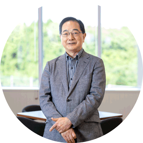
Kiyoshi Ogata | Sr. Executive VP, GM Product Division
Kiyoshi Ogata is a senior executive shaping Rigaku’s global product vision and long-term innovation strategy. With decades of leadership in advanced X-ray technologies and semiconductor metrology, he helps guide the future direction of next-generation characterization solutions and global technology initiatives.
Areas of focus:
- Global product strategy and innovation leadership
- Advanced X-ray instrumentation and metrology
- Long-term technology vision for Materials analysis and semiconductor manufacturing
Markus Kuhn | Executive Officer & Fellow, GM Semiconductor Metrology Division
Markus Kuhn serves as Executive Officer & Fellow and General Manager of the Semiconductor Metrology Division at Rigaku. At FCMN 2026, he is a Program Co-Chair, playing a central role in shaping the conference’s technical vision and advancing collaboration across the nanoelectronics metrology community. He works closely with industry leaders, researchers, and technology innovators to drive dialogue around next-generation characterization challenges and solutions.
Areas of focus:
- Advanced X-ray metrology strategy and innovation
- Semiconductor materials and structural characterization
- Industry–academia collaboration and technical leadership during the conference

Naoki Matsushima | Senior Director of Technology Semiconductor Metrology Division
Naoki Matsushima leads technology strategy and advanced product initiatives for Rigaku’s semiconductor metrology portfolio. He focuses on translating emerging nanoscale measurement challenges into practical, customer-driven metrology solutions while aligning development roadmaps with future device requirements.
Areas of focus:
- Technology strategy and product roadmaps
- Nanoscale dimensional and thin film metrology
- Customer-driven innovation and solution development
Meredith Beebe | Account Manager, West Coast
Meredith Beebe is an accomplished analytical chemist and semiconductor metrology specialist with more than 15 years of experience in X-ray applications and customer engagement. She partners with customers across the West Coast to deliver application-focused insights and build strong, trusted technical relationships.
Areas of focus:
- Semiconductor X-ray metrology applications
- Technical sales support and customer engagement/li>
- Trace metal and thin film analysis/li>

Rodney Chisholm | Account Manager, East Coast
Rodney Chisholm brings more than three decades of experience in semiconductor lithography, technical sales, and global customer support. He works with customers across North America on advanced X-ray metrology solutions, helping address complex materials and process challenges in next-generation device manufacturing.
Areas of focus:
- TXRF, VPD-TXRF, WDXRF, EDXRF, XRR, XRD, HR-XRD metrology
- CD-SAXS, T-SAXS, GI-SAXS and hybrid measurement strategies
- Strategic customer support and global fab engagement

Contact Us
Whether you are interested in getting a quote, want a demo, need technical support, or simply have a question, we're here to help.