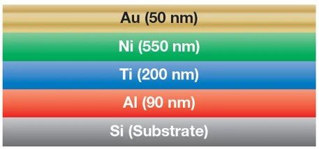
Thickness Characterization of a Power Device Backside Electrode
WDXRF can monitor metal film thickness and uniformity with high precision and throughput.
All four layers, even the bottom Al, can be analyzed simultaneously thanks to the high-power (4 kW) X-ray source and the FP method.

Elements measured by WDXRF
| X Y | Au | Ni | Ti | Al |
| nm | nm | nm | nm | |
| Average (nm) | 49.3 | 551.3 | 198.2 | 89.5 |
| Maximun (nm) | 50.4 | 557.3 | 201.2 | 91.1 |
| Minimun (nm) | 48.1 | 544.8 | 195.3 | 87.9 |
| Range (nm) | 2.3 | 12.5 | 5.9 | 3.23 |
| Sigma (nm) | 0.90 | 3.59 | 1.61 | 0.87 |
| RSD (%) | 1.82 | 0.65 | 0.81 | 0.97 |

Recommended Rigaku semiconductor metrology tools

Contact Us
Whether you are interested in getting a quote, want a demo, need technical support, or simply have a question, we're here to help.
