Application Note B-XRI1034
Additive manufacturing, often referred to as 3D printing, is transforming the way complex parts are designed and built. Its ability to produce intricate shapes, rapidly test prototypes, and utilize a wide range of materials makes it invaluable across many industries. But the same flexibility that makes additive manufacturing powerful also makes it challenging to control. Even small changes in build parameters can affect the final product’s quality in subtle but important ways.
This is where advanced imaging tools come in. X-ray computed tomography (CT) allows us to see inside materials without cutting them open, creating detailed 3D images of both external and internal features. For additive manufacturing, this means engineers can directly link printing parameters to structural results.
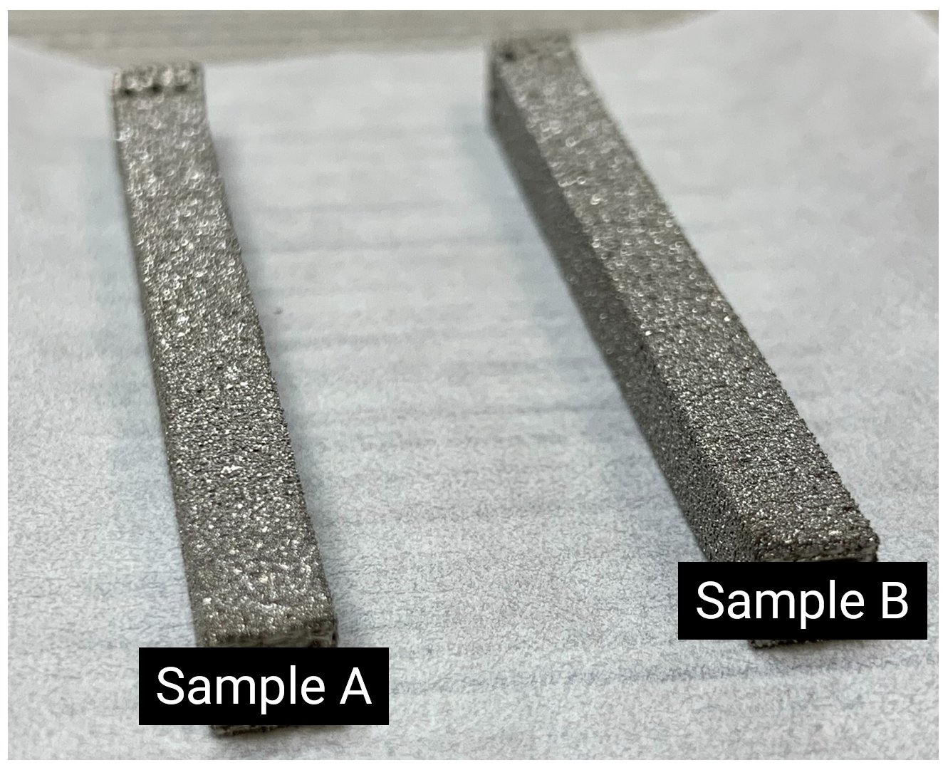
About the sample: Titanium rod samples
In this demonstration, we used CT to analyze two titanium alloy rods, labeled Sample A and Sample B, both manufactured with electron beam powder bed fusion (EB-PBF). They were built from the same Ti-6Al-4V alloy powder, but under different printing conditions.
Although both rods appear similar on the outside, CT can reveal differences hidden within.
Analysis procedure
- Both rods were scanned using the CT Lab HV, a micro-CT system.
- The resulting 3D images were segmented using histogram thresholding to distinguish material from voids.
- Surface roughness was measured by comparing each rod to an ideal smooth reference. Wider deviations correspond to rougher surfaces.
- Internal voids were mapped to evaluate differences in manufacturing quality.
CT scan
Titanium’s high density can create artifacts such as beam hardening artifacts and metal artifacts in CT images. To reduce these effects, the rods were scanned with high-energy X-rays (200 kV, 70 µA) using CT Lab HV, which can operate at up to 225 kV. This produced clearer images, allowing fine internal details to be resolved.
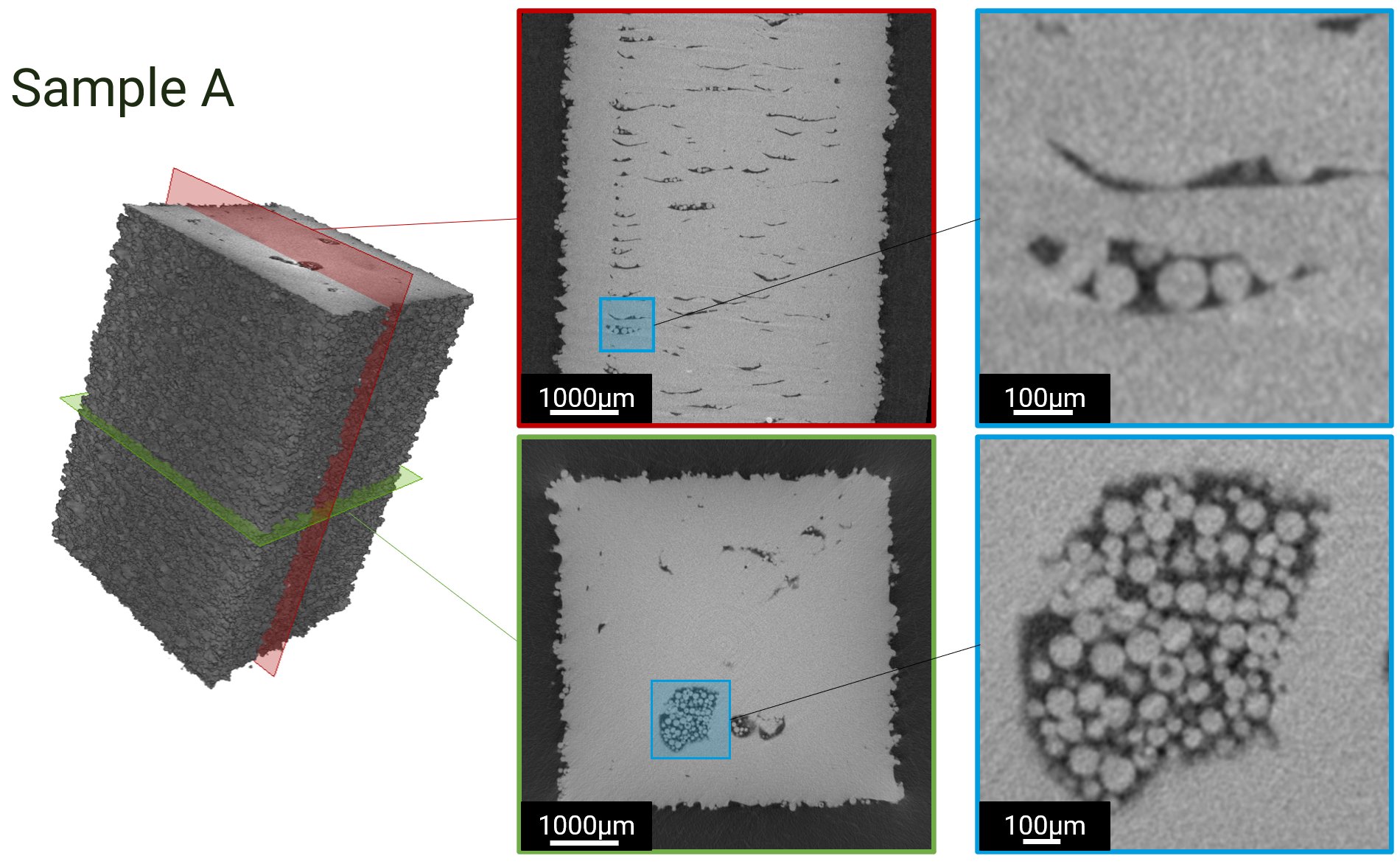
In Sample A, voids between printed layers were immediately visible.
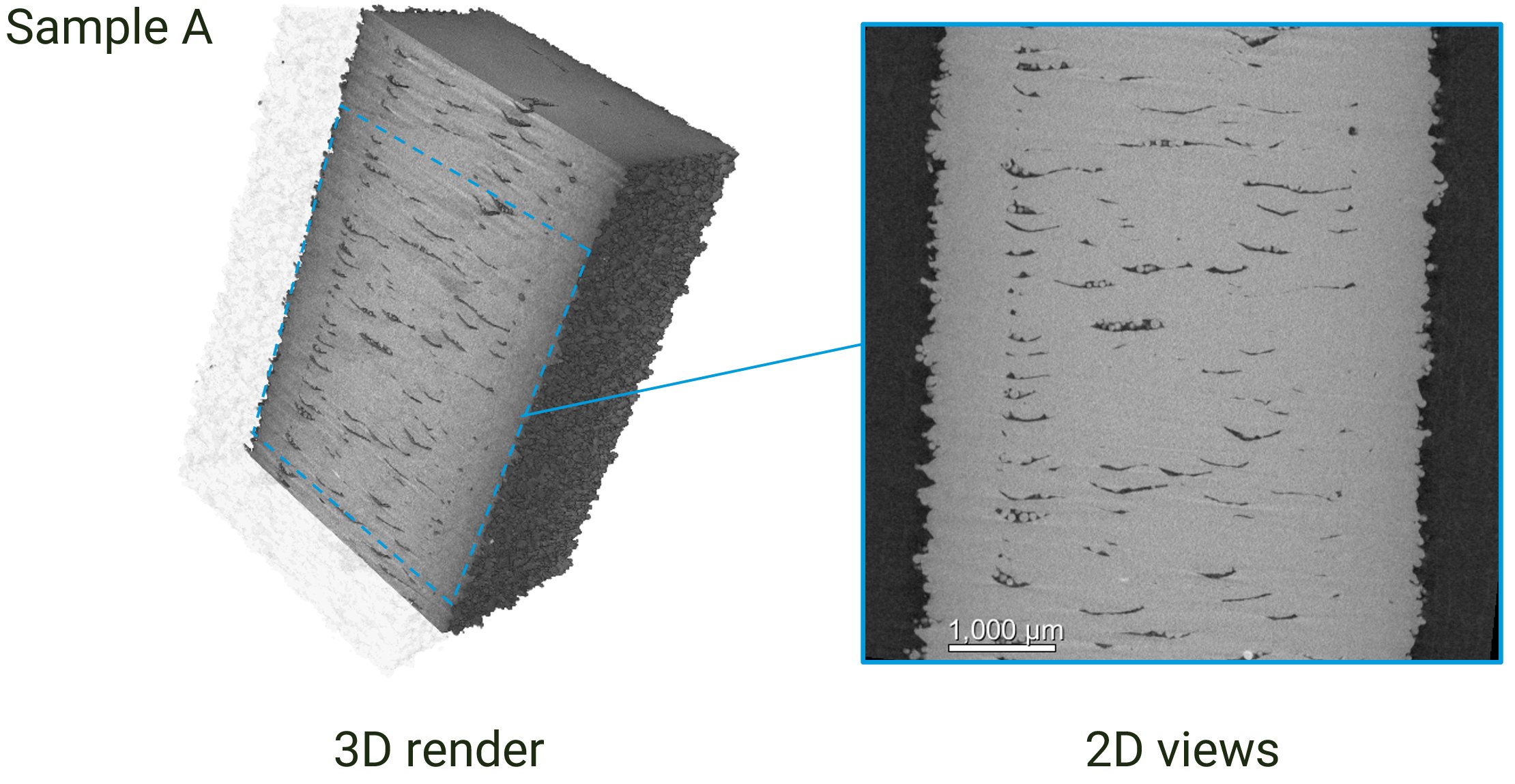
Zooming in further revealed unmelted spherical powders trapped inside larger pores—a sign of incomplete melting during the fabrication process.
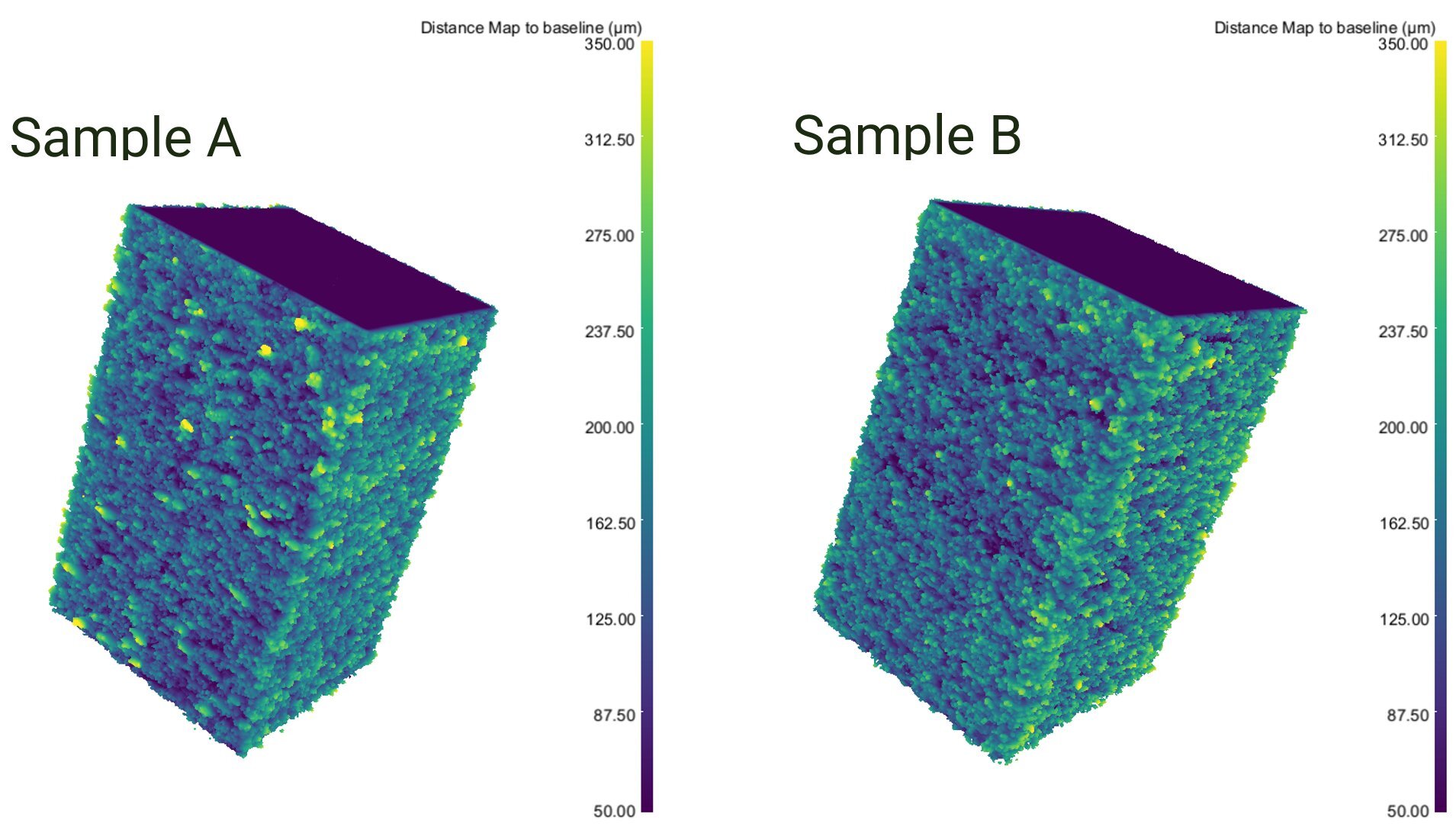
Surface roughness analysis
The high-contrast CT data allowed us to map and measure surface roughness through segmentation on both rods using Dragonfly 3D World. Roughness measured by comparing against an ideal flat surface ranged from 50 µm to 350 µm. Despite different print conditions, both Sample A and Sample B showed similar overall surface roughness and texture, as illustrated in the figure below. This analysis provided not only a visual map of the roughness but also quantitative estimates of the deviation ranges.
Void analysis
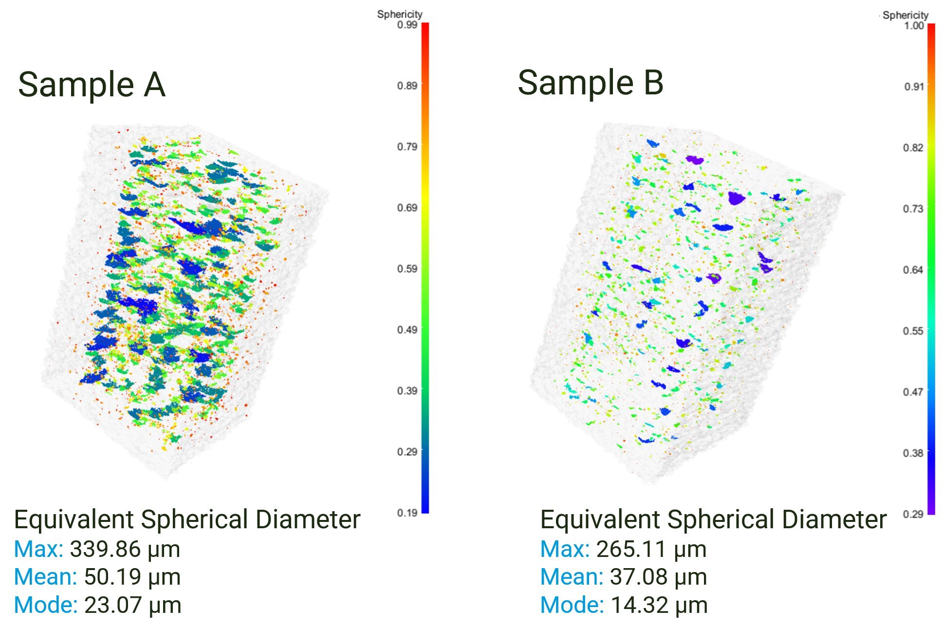
The internal pore structures told a different story. Visualization made it clear that Sample A contained more voids than Sample B. Quantitative measurements confirmed this: porosity in Sample A was 0.55% by volume, compared to just 0.12% in Sample B.
Pore sizes also differed. The largest pore in Sample A measured nearly 340 µm across, with an average size of about 50 µm. In Sample B, pores were smaller, with a maximum of 265 µm and an average of approximately 37 µm. These differences stem from the different process parameters used during the fabrication process.
Sphericity analysis revealed two distinct pore types, as shown in the figure below. Larger, elongated voids (shown in blue-green) were mostly located between printed layers, while smaller, more spherical pores (orange-yellow) were evenly distributed through the material. With CT, these distributions are not only measured but also visualized, making structural differences clear at a glance.
A full 360° video of Sample A illustrates both external and internal features in detail.
Conclusions
This case study demonstrates how X-ray computed tomography (CT) provides a window into the hidden structures of 3D-printed parts. Without damaging the samples, CT revealed surface roughness, trapped powders, and void distributions, all of which are critical to understanding how printing parameters influence final part quality. For additive manufacturing, high-voltage CT offers both qualitative visualization and quantitative data—tools that help refine process settings and improve product reliability.