Examination for Growth Process of Organic Thin Film by In-plane XRD
Introduction
The organic semiconductor pentacene has attracted a lot of attention for potential use in TFT (thin film transistor) due to its high carrier mobility which approaches that of amorphous Si. However, controlling the crystal phase and molecular orientation in the pentacene thin film is essential to obtain optimal characteristics. In this example, we perform phase identification and evaluation of orientation of the pentacene molecules in thin films different in thicknesses as well as crystallite size determination.
Measurements and results
Pentacene thin films 150 nm and 20 nm thick were deposited on silicon substrates using MBE (Molecular Beam Epitaxy). The Si 100 substrates also had a 300 nm thick SiO₂ thermal oxide layer. Figure 1 shows the out-of-plane XRD (θ/2θ scan) profile and Figure 2 shows the in-plane XRD profile(1). 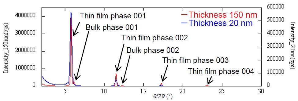 Figure 1: The out-of-plane XRD profile for pentacene thin films (The diffraction from lattice planes parallel to the sample surface).
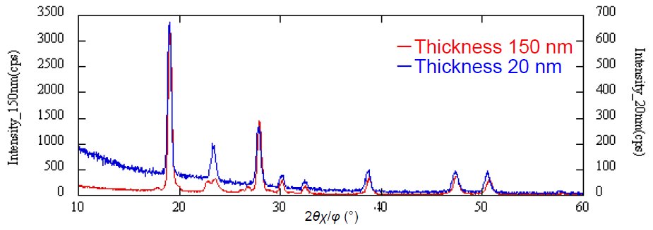 Figure 2: The in-plane XRD profile for pentacene thin film (The diffraction from lattice planes perpendicular to the sample surface).
In the out-of-plane X-ray diffraction profile, only the pentacene 00l reflection was observed, while in the in-plane X-ray diffraction profile, only the pentacene hk0 reflection was observed. These results indicate that the pentacene c-axis was oriented normal to the sample surface in both samples. In the 20 nm pentacene thin film, only the diffraction peak of the thin film phase having the 15.40 Å c-axis was observed, whereas in the 150 nm thin film, additional peaks of the bulk phase having 14.40 Å c-axis was detected as well(2),(3). These results suggest that the phase seen in the 20 nm film grows first, and then the phase in 150 nm film grows as the film thickness increases.
The crystallite size in the in-plane direction was determined by using the thin film phase 100 peak at 2θ = 19° observed in the in-plane diffraction profile. The Scherrer method estimated crystallite size to be approximately 50 nm for both samples. Thus, we found that the crystallinity in the in-plane direction was constant regardless of film thickness.
Samples provided by: Saiki laboratory, The University of Tokyo.
References
(1) K. Inaba: Rigaku Journal (English version), 35(1) (2004), 27-36.
(2) C.C. Mattheus, et al.: Acta Crystallogr., C57(2001), 939-941.
(3) J.S. Wu and J.C.H. Spence: J. Appl. Crystallogr., 37(2004), 78-81.

Contact Us
Whether you're interested in getting a quote, want a demo, need technical support, or simply have a question, we're here to help.