Background
Silicon carbide is used for blue LEDs, ultrafast high-voltage Schottky diodes, MESFETs and high temperature thyristors for high-power switching. By growing SiC thin films on Si, it can be naturally integrated with the mature Si technology. Growing high quality, defect-free SiC thin films is essential for their applications. High-resolution triple-axis X-ray diffraction provides a nondestructive, quick, and quantitative measure of the film quality and possible defect density.
Investigation
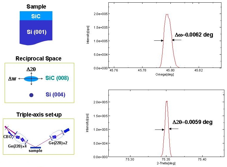
In the figure below, both ω and ω/2θ profiles around the (008) Bragg point of a 200nm SiC thin film on a Si (001) substrate measured on the SmartLab diffractometer are shown. By using the triple-axis configuration, consisting of a Ge(220) 4-bounce monochromator and a Ge(220) 2-bounce analyzer, the widths of the SiC reciprocal lattice point along the in-plane and the out-of-plane directions were measured separately. The in-plane width (Δω) typically relates to mosaic spread or misfit dislocation density; whereas, the out-of-plane width (Δ2θ) relates to the variation of lattice constants due to, for example, composition variation. The narrow in-plane and out-of-plane peak width of the sample shown here indicate that the film is of excellent quality.