Background
In a high dielectric-constant (high-k) ultra-thin oxide insulation film that is required in the next generation semiconductors, it is indispensable to evaluate whether certain crucial characteristics are created as expected during the fabrication process. Among these traits are the film thickness, the absence or presence of intermediate layers and the state of crystallinity. From X-ray reflectivity measurements using Rigaku's SmartLab multipurpose diffractometer the film thickness, density and interface roughness of an insulation film of more than about 1 nm can be evaluated in a laboratory.
Investigation
The figures below show the reflectivity measurement results of a 5 nm ZrO2 thin film formed on a Si substrate. By analyzing the reflectivity profiles in detail, the presence of the interface layer and its thickness can be evaluated. The analyzed results reveal that the thickness and density of the ZrO2 thin film are 4.215 nm and 5.233 g/cm3 respectively, roughly the same as the designed values. A ZrOSi layer is present in the interface layer and its thickness and density are 1.383 nm and 3.188 g/cm3, respectively

|

|
In the in-plane method, in which X-rays enter the sample surface at a glazing angle, it is possible to perform a diffraction measurement for films as thin as 1 nm thick. The figures below show the diffraction profiles of 1 nm, 5 nm and 10 nm thick ZrO2, respectively. In the 1 nm thick ZrO2, the figure reveals that crystallization slightly occurs after forming an amorphous layer at the as-deposited state and annealing it, and that a crystallized film can be formed even at the as-deposited state.
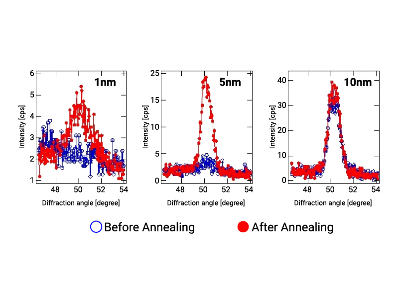
Samples provided by TOSHIBA Semiconductor Co. and TOSHIBA Nanoanalysis Co.