Background
Due to quantum effects, epitaxial III-V semiconductor nanostructures promise better optoelectronic devices, such as LEDs, lasers, and detectors. Self-assembly is probably the most efficient and low-cost technique to grow such nanostructures. Accurate characterization of the strain distributions—as well as the size and shape—of the nanostructures is crucial to understanding the growth mechanism and hence to the improvement of their quality.
Investigation
High-resolution X-ray reciprocal space mapping has proven a powerful technique for the study of epitaxial nanostructures, including quantum wells, wires, and dots. SmartLab®'s variable resolution optics allow fast measurement of such nanostructures at medium, high, or ultra-high resolutions. Below is a (004) reciprocal space map (displayed in both 3D topograph and 2D contour) taken from a 2D InAs nanowire array with GaSb spacers grown on a GaSb substrate by molecular beam epitaxy (MBE). A high-resolution setup with the combination of a Ge(220)*2 monochromator and a Ge(220)*2 analyzer was used to achieve sufficient resolution for this measurement.
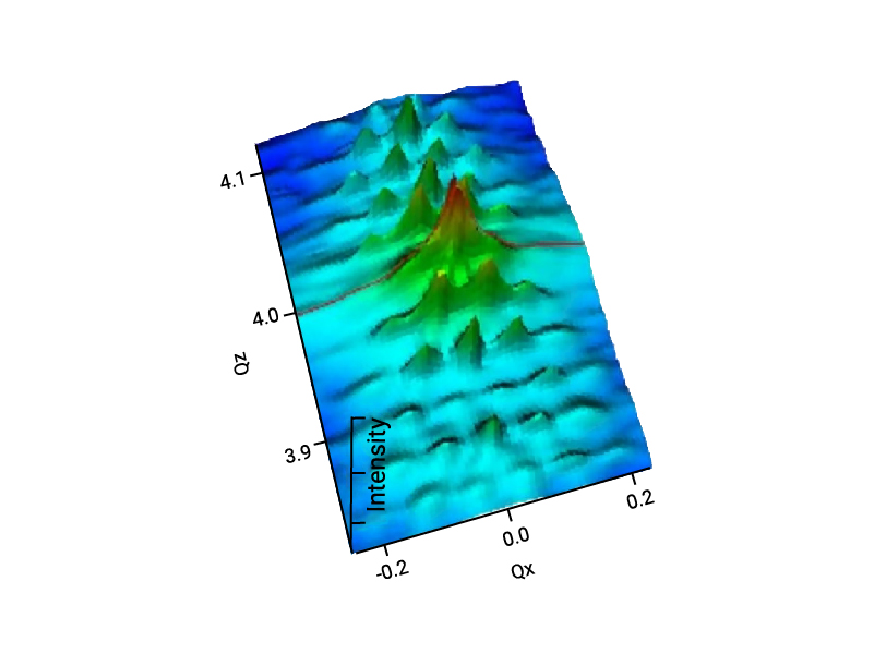
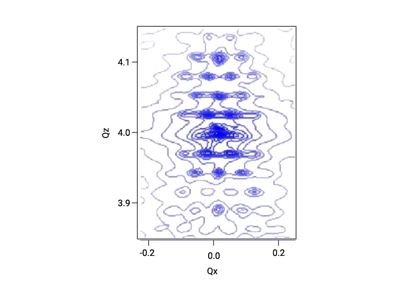
The appearance of the high-order 2D satellites in the map clearly indicates that the InAs nanowires form a well ordered 2D lattice with a face-centered rectangle symmetry. From the positions of the satellites, it is determined that this 2D rectangle lattice is 120 nm wide and 16 nm high. Further information, such as strain distribution, can also be obtained from the satellite intensities by performing rather complicated model calculations.